


Printed Circuit Board Gerber Files

Gerber files are a key piece to the puzzle for manufacturing printed circuit boards. They contain all the necessary data that a PCB manufacture will require to produce the boards to your exact specifications accurately. AdvancedPCB offers free tools like our PCB Artist Design Software simplifies the way you transfer your design files to us for fabrication. Our FreeDFM Gerber file check tool is another way AdvancedPCB makes it easier to ensure all your files are complete before placing your order.
In this post, we discuss the basics of printed circuit board Gerber files. For more detailed information about Gerber file generations and our requirements, click here. For more PCB design and manufacturing resources, visit our PCB Engineering & CAM Resources page.
What are PCB Gerber Files
A Gerber file is basically an image of a PCB. It showcases each individual layer as it appears throughout your circuit design. Gerber files represent copper layers images, solder mask, legend, and drill and route data helping to simplify the process of seeing how the circuit board should be fabricated. The Gerber files also contain attributes that provide meta-information about these images, such as whether a graphics object is and SMD pad, a via pad, a fiducial, or any other type of element.
Multiple programs have the ability to read a Gerber file format due to its simplicity, yet detailed descriptions of its contents. They additionally assist in locating potential issues and debugging of the circuit design when uploaded to our FreeDFM file check tool. When submitting a Gerber file, it is wise to send a straightforward text (.txt) file with the explanation of the requirements that may not appear in the file as a note to the PCB manufacturer.
What’s Included in PCB Gerber Files
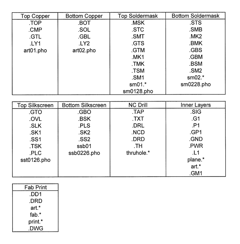
When exporting the set of Gerber files for your PCB design, you will notice there is a set of individual files with different extensions which should be saved as a zipped folder to send over to the PCB manufacturer. These files are the following elements of your circuit board design:
- Top Silkscreen
- Top Soldermask
- Top Copper
- Top Solderpaste
- Inner Copper
- Bottom Copper
- Bottom Soldermask
- Bottom Silkscreen
- Bottom Solderpaste
- NC Drill
- Non Plated Drill
- Slots
- Drawing/Other
When submitting your files for PCB fabrication, you will need to map your files (match) to the elements mentioned above. Common file name extensions are listed in the image below.
.jpg "gerber-files-768x778-(1).jpg")

AdvancedPCB
Related Posts

How to Better Plan Your Printed Circuit Build

How to Improve Your PCB Design
