


PCB Design Services
PCB design is the process of turning an electrical schematic into a physical printed circuit board (PCB) that can be manufactured and assembled. AdvancedPCB's design services include assistance in selecting materials, defining the PCB stackup, placing components, routing traces, managing power and ground, and verifying that the board will meet electrical, mechanical, and regulatory requirements.
PCB design is available as an additional service through AdvancedPCB; design work is not performed at our manufacturing facilities.
High-Speed PCB Design Services
As data rates increase, so does the need for transmission speed. This can drive signal integrity (SI) issues such as crosstalk, reflection, and signal loss. At the same time, many products incorporating dense high-speed digital circuitry have rapid product development cycles, which do not allow for the multiple iterations that can be driven by use of an inexperienced design team.
AdvancedPCB’s team of IPC CID+ designers specializes in tackling these challenges. Our skilled DFM Engineers collaborate with your PCB design and product development teams. Our comprehensive approach to circuit board design services and PCB layout services ensures:
- Routing strategies focused on controlling impedance and crosstalk.
- Industry-standard layout techniques to optimize signal integrity.
- Best-in-class materials for optimal PCB stackup and power requirements.
- Close coordination with product development engineers to meet all requirements.

High Density Interconnect (HDI) and RF PCB Layout Services
As the size of circuit boards decrease and functionality increases, dense packaging challenges arise, often involving blind and buried vias, laser microvias, and complex stackups. Our team, skilled in EMI principles, collaborates with engineers to maintain signal and power integrity in high-density PCB design and advanced PCB design services.
Key elements of effective HDI printed circuit board layout services include:
- Matching the right tools and designers to specific product needs.
- Continuous learning of industry-standard practices and design rules.
- A collaborative approach aligning resources with development timelines.
- Expertise in stackups and via technology for complex routing.
Rigid-Flex and Flex PCB Design
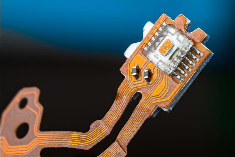
The growing trend of interconnected products and shrinking sizes drives RF technology to use rigid-flex circuitry, posing design challenges. Our team addresses these with industry-standard design rules and decades of expertise in PCB board design and PCB layout services.
The AdvancedPCB design team excels in translating product requirements into functional layouts with RF engineers; ensuring design meets functionality and manufacturability requirements; and using a collaborative process to reduce layout time and design iterations.
Whether you need us to design PCBs from the ground up or refine an existing PCB circuit board design, our circuit board design services keep performance and reliability at the forefront.
Signal/Power Integrity in PCB Design
Achieving optimal printed circuit board layout requires a team that offers various options for price and performance. AdvancedPCB’s senior designers provide this flexibility, ensuring the best layout and fabrication strategy. Our PCB design services cover everything from early concept PCB design to final PCB circuit board design verification.
Our analysis tools and practices include:
- Signal integrity routing best practices by experienced designers.
- Power integrity management through materials, vias, and circuit design.
Through these circuit board design services, we help design PCBs that maintain robust power delivery, low noise, and consistent performance across demanding operating conditions.
PCB Design Services by Application Area
Aerospace & Defense
AdvancedPCB provides circuit board design services for aerospace and defense, including applications like:
- Aerospace cockpit instrumentation
- Cyber security systems
- Satellites and telemetry
- Missile computers and communications
We adhere to certifications such as MIL-PRF-31032, IPC 6012 Class 3/3A, and AS9100D, ensuring our PCB design and PCB board design processes meet stringent reliability and quality standards.
Commercial & Enterprise
Partner with an industry leader for PCB layout services and PCB design services across sectors like medical, automotive, and networking. Our capabilities include:
- Blind and buried vias
- Up to 40 layers and heavy copper
- Multilayer RF designs and oversized boards
From initial circuit board design to final printed circuit board layout services, we support complex commercial products that demand high reliability, manufacturability, and cost-effective production. Our team can design PCBs tailored to your stackup, mechanical, and regulatory constraints.
Additional PCB Design Resources
For recommendations and insights on PCB design, read these relevant blog articles:
- How to Make the PCB Assembly and Design Process Flow Smoothly
- Top Advantages of Prototyping for PCB Design Success
- Common PCB Design Mistakes
- PCB Design and Layout Tips: What You Should Know