A step-by-step guide to building a standard rigid, multi-layer PCB
.png?resizemode=force&maxsidesize=500)
Printed circuit board fabrication is a multi-step manufacturing process that transforms digital design files into a functional, electrically tested PCB. While advanced builds like HDI, rigid-flex, and filled-via constructions add complexity, the foundation of PCB manufacturing follows a consistent workflow. Understanding this standard rigid, multilayer PCB fabrication process helps design engineers create manufacturable layouts, reduce risk, and avoid costly respins.
This guide walks through each major fabrication step for a standard rigid multilayer PCB with plated through-holes, explaining how customer data is converted into production-ready hardware.
The steps required to fabricate a PCB can grow in complexity from standard rigid, multi-layer circuit boards to high-density interconnect (HDI) or flexible PCBs. The process can feel confusing when faced with a slew of industry-specific jargon and vendor-specific software. This tutorial defines the fabrication process for a standard rigid, multi-layer PCB, highlighting how the received customer files are converted into a working board.
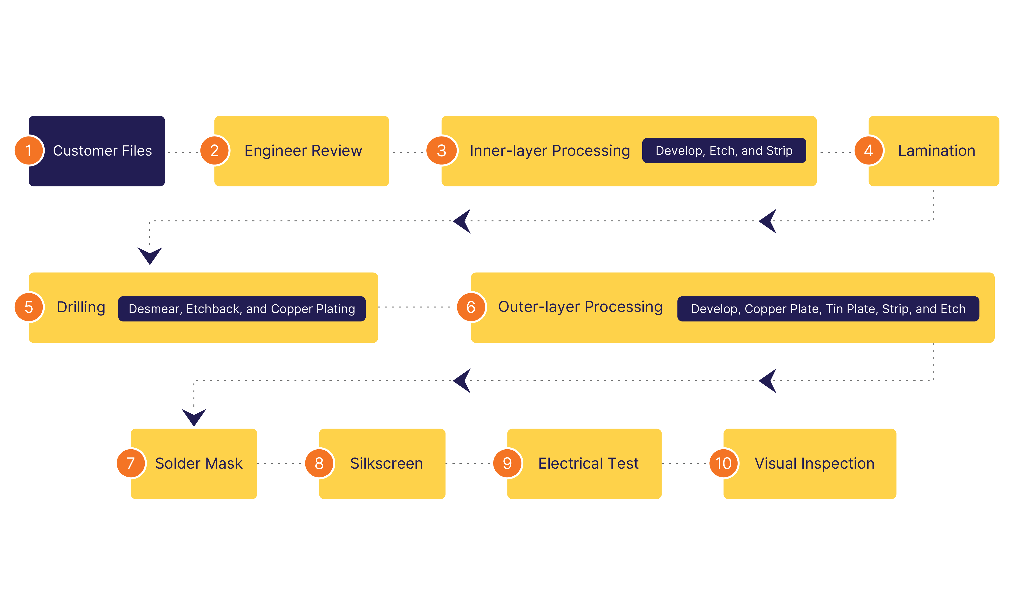
Figure 1 shows a flow diagram of the steps in fabricating a PCB. Note that this does not include more complex processes, such as tented or filled vias.

Figure 1: The PCB fabrication process for a standard rigid, multilayer PCB with simple, plated through-holes.
From Customer Design Files to Manufacturing Data
In the first step, the received customer files come in different formats, including ODB++, IPC-2581, or the most common: the standard Gerber files (RS-274-D). The IPC pushed for a single industry standard that allows data to be seamlessly transferred and used throughout the production process, making IPC-2581 more popular over time. The engineering team will review these files; computer-aided manufacturing (CAM) and planning are done for the particular PCB manufacturing.
The files are sent for an engineer’s review to ensure they are manufacturable and that there are no flaws that could ruin an entire batch of boards. The engineer selects the base material and a panel size (each PCB facility will generally have various standard panel sizes from which to choose). The base materials are a mix of rigid materials, such as laminates and prepreg sheets, and copper foil. Prepreg sheets are loosely woven glass fabrics that are “pre-impregnated” with uncured resin; these do not include copper on either side. Composed of resin and glass fabric with copper on either side, the laminate cores are already cured. Laminate cores effectively employ one or more prepreg laminates pressed under heat and hardened. Standard PCBs use the common FR-4 material.
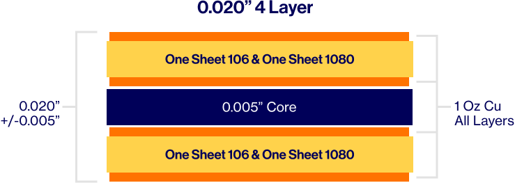
If prepreg sheets are deployed as well, engineering determines the stackup, in which the end thickness depends on the style of prepreg material, the thickness of the copper foil, and the laminate core (Figure 2).

Figure 2: Standard 4-layer PCB dimensions with 1-ounce, all-copper layers.
In addition, manufacturing “travelers” are created during this step. The travelers are physical documents that accompany the board at each manufacturing step to track progress and offer critical PCB information, such as routing specifications, raw materials, and quality checkpoints. The IPC Class 2 standard provides the default if the customer does not assign a particular requirement. Throughout the process, inspection points are used to verify the acceptability of the panels.
Inner-layer Imaging and Etching
Fabrication involves inner- and outer-layer processing and finalizing the board with tin plating and a solder mask. For the inner layers, the material is issued and prepped; the core laminate is cleaned with an acid dip and the substrate is coated with a photoresist. At this point, the pattern exported from the computer is transferred to the resist coat, revealing a polymerized pattern in the resist. The board is then placed in a developer solution, which removes unnecessary resist. As a result, the required circuit pattern is visible in photoresist, where the surrounding copper needs to be etched away. This etching is often accomplished with a ferric chloride bath, removing the exposed extra copper and leaving the resist/copper circuit pattern. The resist is finally stripped for the desired circuit pattern in copper. A completed inner layer will show the same image placed on a panel in an array. All inner-layer cores pass through automated optical inspection prior to being laminated into a multi-layer board. Cross-section analysis is used to verify the plating thickness on the surfaces and in the hole walls.
Lamination of Multilayer Boards
After all the inner layers have been finished, the surface of each layer is roughened through an oxide process to promote adhesion during lamination. Lamination involves stacking all the layers according to their original design and squishing them together in a press. Lamination entails the systematic stacking of each layer per its original design, followed by the application of pressure through a press to achieve cohesion. These follow press cycles that specify the level of pressure and heat applied over an allotted time.
Drilling and Hole Preparation
The next step is to create vias by drilling holes through the PCB. These can be used either to mount components by their leads or to ensure the individual layers of the board can be lined up in multi-layer PCBs. First, the board is X-rayed to check its registration, ensuring the layers are perfectly aligned before drilling. Then the drilling can begin.
Drilling comes with a couple of considerations. The drill itself would melt the resin and cause it to run up and down the vias, preventing the necessary copper plating. This requires them to be cleaned with either a desmear or etchback process. After the holes have been cleaned, electroless copper plating is used to deposit a layer of copper in the holes. The plating can be built up to a specific thickness via electrolytic copper plating. After this, the outer layer is finally processed, leaving the final copper pattern and finished board. The outer-layer process is almost identical to the inner-layer process.
Outer-Layer Imaging and Plating
Outer-layer processing mirrors inner-layer imaging but incorporates copper plating to form the final conductor thickness. Photoresist is applied, imaged, and developed, followed by copper and tin plating. The remaining resist is stripped, and unwanted copper is etched away, leaving the final external circuit pattern.
Solder Mask and Silkscreen Application
The final steps involve the solder mask and silk screening, wherein the liquid solder mask covers the vias to protect them when soldering is performed on the PCB. The silkscreen is applied on top of the solder mask by inkjet-printing names, numbers, symbols, part identification information, and other text elements on the board.
Final inspection and Electrical Test
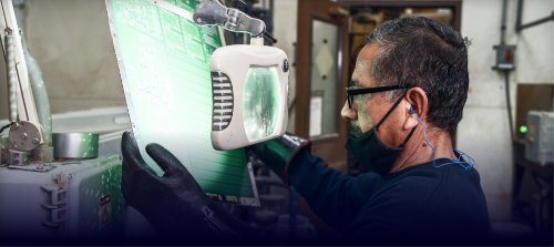
During the final inspection, the board undergoes a standardized inspection process (Figure 3). Each order is subjected to C=0 random sampling to ascertain that the holes and dimensions for each part number conform to specified tolerances. After the order has passed the dimensional check, it is scheduled for an electrical test, depending on its requirements. The last step for each order is a 100% visual inspection: Each part is checked for workmanship, quality, cleanliness, and other attributes before the boards are packaged for shipping.

Figure 3: The board undergoes a standardized inspection process.
Summary
The process of fabricating a PCB involves many intricate steps. Therefore, the wrong move and poor planning could produce a domino effect that can lead to a non-functioning board or one that is not up to spec. To mitigate the risks of a high-volume order, work with an experienced manufacturing facility that offers the proper infrastructure, from certifications to equipment. AdvancedPCB offers the legacy and expertise to troubleshoot and manufacture standard to more complex PCBs in small and large volumes quickly.
______________________________________________________________________________________________________________________________________________
Frequently Asked Questions
What file format is best for PCB fabrication?
IPC-2581 is the most comprehensive file format because it combines fabrication, assembly, and test data into a single intelligent data set, reducing translation errors. However, Gerber (RS-274X) files are still widely accepted and commonly used. Most PCB manufacturers support both, along with ODB++.
How long does it take to fabricate a standard multilayer PCB?
Fabrication time depends on layer count, materials, and complexity. A standard rigid 4-layer PCB typically requires 5–10 business days for fabrication, while expedited or quick-turn builds can be completed in as little as 24–72 hours, depending on technology and capacity.
What IPC standard applies if no PCB class is specified?
If no acceptance class is defined by the customer, manufacturers generally default to IPC Class 2, which covers most commercial and industrial electronics. High-reliability applications, such as aerospace, defense, and medical devices, often require IPC Class 3 for tighter tolerances and increased reliability.

AdvancedPCB
Related Posts

How Integrated PCB Fabrication and Prototype Assembly Improves Speed and Program Control

Prototype PCB vs. Full Spec Production: A Guide for Design Engineers


