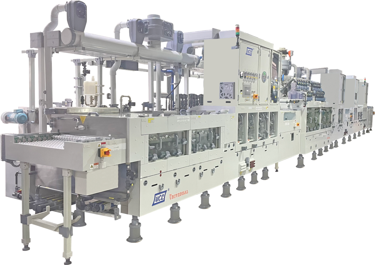
AdvancedPCB Bolsters Manufacturing Capabilities with New SES (Strip-Etch-Strip) Wet-Process Line
Posted
9/25/2025


AdvancedPCB is pleased to announce the deployment of a new SES (Strip-Etch-Strip) wet-process line as part of its continued investment in core manufacturing infrastructure. This new line strengthens AdvancedPCB’s in-house wet processing capabilities, improving throughput, process control, and reliability. All of which translate into better service and consistency for our customers.
The SES process is a key stage in PCB fabrication, combining successive strip, etch, and strip operations into a streamlined, continuous wet-process line. It is especially critical for outer-layer pattern definition, film stripping, and preparing copper surfaces for further processing. SES lines are instrumental in reducing film residue, improving etch uniformity, and optimizing chemical usage.
By integrating film stripping and etching steps, SES lines help reduce cycle times, lower handling, and maintain tighter control over the surface quality, a crucial advantage when working with fine-line, high-density designs.
What This Means for Our Customers
While the technical details of the machine are important, our focus is always what these investments mean for you:
- Faster throughput through reduced process step transitions
- Greater consistency & yield via tighter control over chemical and stripping processes
- Enhanced quality assurance as each step is more reproducible and integrated
- Scalability and flexibility to support more demanding designs and increased volume
As always, our guiding principle is service: our technology investments are meant to support improved turnarounds, higher confidence in every board, and more predictable execution for your projects.
Browse
All Categories
Recent Posts
View Recent Posts


