An introduction to PCB stencils and their uses

While Advanced PCB (APCB) offers assembly services to populate its bare PCBs, many engineers vote to assemble their PCBs in-house with a PCB stencil. Essentially a flat material sheet, these stencils have an opening cut out for SMT component pads in the unique PCB design. Instead of manually applying solder paste to each individual design pad with a solder paste syringe, solder paste can be “squeegeed” across the stencil sheet over the board, leaving a solder track conveniently laid out over the SMT component’s pad. A basic stencil walkthrough can be seen in Figure 1. This might seem simple enough, but there are a few nuances — solder paste, stencil material/thickness, stencil types, and stencil hole size — that might leave engineers baffled. This tutorial will guide those looking to apply stencils to their design for low-volume board “stuffing”.
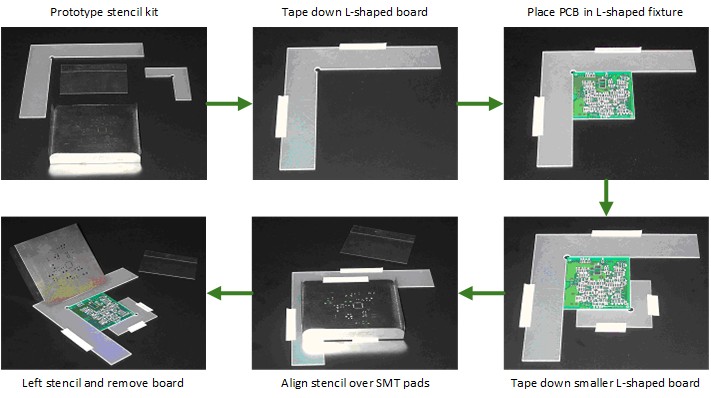
Figure 1: Walkthrough for using APCB’s basic prototype stencil.
PCB Assembly Tools
Choosing a manual or automated approach can determine the tools engineers and technicians will need for their PCB assembly:
-
Solder paste
-
Syringe or automated syringe
-
Frameless, framed, glue-in, or mounted stencils
-
Paste application machine (e.g., manual/automatic stencil printer) or squeegee (e.g., credit card, razor blade, putty knife, etc.)
-
Tweezers, pick-and-place tool, or pick-and-place machine
-
Heat gun, hot air soldering station, or reflow oven
Solder paste
Solder paste combines flux and small metal fragments (solder) used to apply the electronic components to the printed circuit board. Flux is a chemical that assists in the metal’s bonding and melting.
Solder paste syringes
Solder paste syringes are useful in manual solder general applications. Force instance, Hybrid PCBs with SMT and through-hole (TH) components use a solder paste syringe — if the overprinting or double printing technique cannot be utilized — to manually apply solder in a pin-in-paste (PiP) or intrusive reflow solder technique. While automated syringes can also apply solder paste, this is more time-consuming than using a stencil.
Stencil
The stencil itself can be framed or frameless. A framed stencil permanently mounts within a frame, while a frameless stencil is a laser-cut stencil without the surrounding frame. APCB frameless, prototype stencils have two L-shaped board fixtures, ensuring that the PCB’s square edge aligns with the L-shaped frame and tapes in place. Frameless stencils, where the stencils do not need to be permanently glued into the frame (Figure 2), are also offered for universal frames such as SMT, QTS, Pro Frame, and Zelflex. APCB offers framed, glued-in, or mounted stencils for high-volume screen printing. For a framed stencil, the stencil is mounted to either a cast or extruded aluminum stencil frame using a mesh border to keep the stencil taut against the PCB panel. The glue-in stencils are permanently bonded to the border for a much stronger bond.
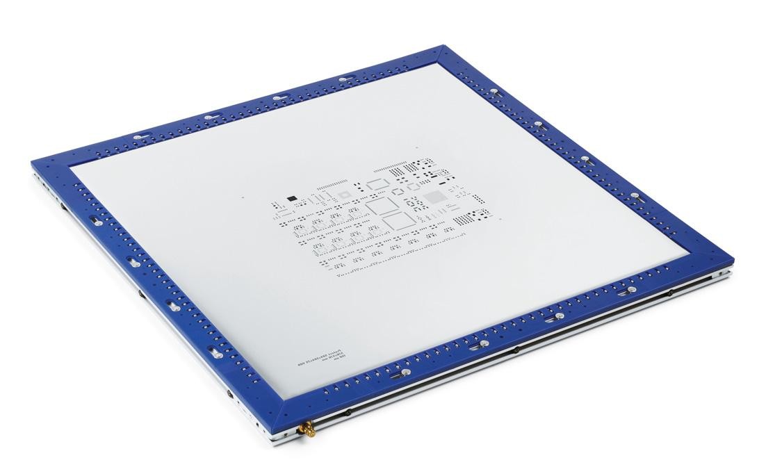
Figure 2: The ZelFlex stretching frame that uses pneumatics to press the stencil down onto the panel, removing any potential bowing. Source: ZelFlex
Solder paste application methods
Using a solder stencil and a paste application machine, solder paste is distributed in exact amounts on the SMT component’s pads (Figure 3). If an automatic machine is not available, this must be executed manually with the utmost precision — particularly the case for extremely fine-pitch components such as BGAs, QFP, or QFN packages, and small chip sizes such as 0402 and 0201 components. Many engineers will use a squeegee for solder paste application. Naturally, there are many considerations that come with manual solder paste spreading with the use of a do-it-yourself (DIY) squeegee such as a credit card, razor blade, or putty knife. The main consideration here is applying consistent pressure across the PCB to distribute the paste evenly, which often requires holding the squeegee at an angle.
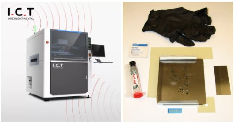
Figure 3: Stencil and solder paste application methods can vary from advanced automatic stencil printers (ICT on left) to basic prototype stencils (APCB right).
Placing components
At this point, it is required to place the SMT components in their respective positions. While this can be done rapidly and accurately with a pick-and-place machine, it is often not an affordable option for low quantity, prototype assembly. As a result, many engineers may want to manually perform this task. If this is the case, use a pick-and-place tool (Figure 4) or a humble pair of tweezers.
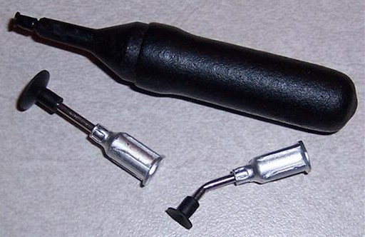
Figure 4: Pick-and-place tool offered by APCB for low-quantity prototype assembly. This tool uses a vacuum bulb and vacuum clips to lift and place SMT components.
Reflow soldering
Finally, heat the boards to ensure the solder melts and reflows to wet the component leads and fuse them to their respective pads after cooling. It is critical to have an accurate reflow temperature profile, as shown in Figure 5. Peak temperature achieves reflow — where the flux reduces the surface tension at the metallic joints to form the solder joint. Naturally, it would be difficult to accomplish an accurate temperature profile with a heat gun; however, it is possible and entirely feasible for one-off boards. While you can alternatively utilize desktop hot-air soldering stations to simplify this process, reflow ovens remain the state-of-the-art option for accurate and precise assembly.
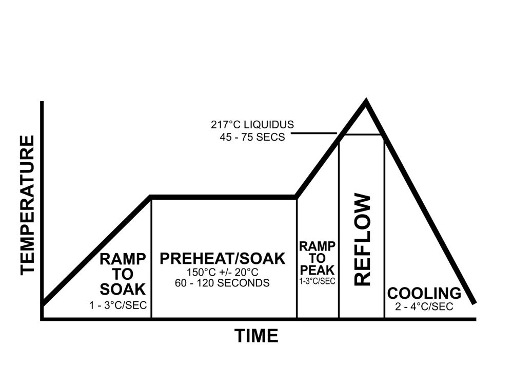
Figure 5: Example of the reflow thermal profile. Source: Wikipedia
Stencil application considerations
Laying stencil flat against the PCB
Application considerations vary based on the employed SMT component’s pitch and size. Stencil application setbacks stem from the stencil and panel’s natural bowing. This prevents the stencil from laying perfectly flat against the panel itself, causing the solder paste to sneak into the stencil’s apertures — potentially causing PCB parts to require reworking. If this is the case within a relatively large production run, it could result in an inordinate amount of reworking that leads to far less efficient production. Consider this for medium- to high-volume PCB production, where framed or glued-in stencils might offer more precision.
Stencil thickness
Stencil thickness, particularly for smaller-size and smaller-pitch components, is another serious consideration. The IPC-7525 stencil guidelines have equations for the required aspect ratio (Equation 1 and Equation 2) and area ratio for stencils with rectangular apertures (Equation 3), and stencils with circular apertures (Equation 4). The variables in these aperture geometries are seen in Figure 6. As the area ratio increases, so does the transfer efficiency — the percentage of solder paste printed into the PCB pad through the stencil aperture.
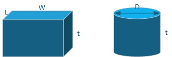
Figure 6: Variables for various aperture geometries.
Aspect ratio for rectangular aperture=Aperture width (W)Stencil thickness (t)>1.5 (1)
Aspect ratio for circular aperture=Aperture diameter (D)Stencil thickness (t)>1.5 (2)
Area ratio for rectangular aperture =Area of opening (LW)Area of aperture walls (2t(L+W))>0.66 (3)
Area ratio for circular aperture =Area of opening (D24)Area of aperture walls (Dt)=D4t>0.66 (4)
As the opening area decreases to accommodate the decreasing pad sizes of fine-pitch components, so too must the aperture wall area. Essentially, the thickness must decrease to maintain the same transfer efficiency. A 0201 part is 10 mils wide and 20 mils long (0.3 mm x 0.6 mm), calling for 5 mil (0.12 mm) thick stencil sheets to maintain an area ratio greater than 0.66 (0.83). Thinner stencils have other benefits: they require less solder paste volume and tend to release the solder paste when lifted from the PCB, as opposed to taking the solder paste and removing it from the pad.
APCB’s stencils are 100% laser-cut, stainless steel type 304 (T304) with stencil thicknesses ranging between 4 and 7 mils. Naturally, employing different materials can achieve stencils for solder paste printing. Laser-cut stainless steel, however, has become the most popular choice due to its precise thickness control, cost-effectiveness, and corrosion resistance.
Solder paste type
Solder paste should also follow the “five ball rule,” where the stencil’s aperture width houses at least five of the solder paste’s largest particle diameter (Figure 7). The IPC J-STD-005 standard lists the solder paste particle sizes, in which the largest particle diameter ranges from 150 µm for Type 1 (T1) pastes to 20 µm for Type 6 (T6) pastes. Many engineers prefer T5 pastes in finer apertures, while using T3 pastes for wider apertures.
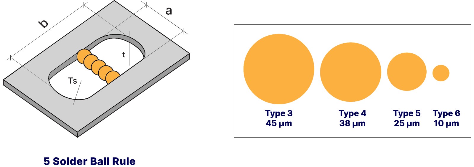
Figure 7: The five-ball rule and largest particle sizes for Type 3 to Type 6 solder pastes, in accordance with the IPC J-STD-005 standard.
The methodology behind applying solder paste to all component pads on a bare board can be complex. Considering the type of required solder paste comes first, then selecting the preferred stencil and application method. Framed and frameless stencils each have their own respective consideration to take into account. While feasible in small volumes, PCB assembly and solder reflow can be time-consuming, error-prone tasks. Ultimately, it is up to the engineer to decide on the precise assembly method. Whether the engineer would like to manually perform the job in its entirety, use APCB to assemble a partial board, or use APCB to fully populate a bare board, APCB has a number of tools to help with each process. APCB assembly builds to IPC-A-610 Class 2, where Class 3 and J-STD-001 are available with prior review. For more information, visit https://www.advancedpcb.com/en-us/services/assembly-services/.
Related Posts

Prototype PCB vs. Full Spec Production: A Guide for Design Engineers

2-Layer vs. 4-Layer Printed Circuit Boards: How to Choose the Right Option


