Avoiding common pitfalls in designing Flex PCBs

Introduction
Flex and Rigid-Flex boards can reduce both the size and weight of an electronic solution by replacing bulky wire harnesses. To facilitate movement of the application, traces are routed across the Flex or Rigid-Flex assembly to bend or twist, with the complex “bookbinder” construction (Figure 1) enabling repeated bends on a certain axis.
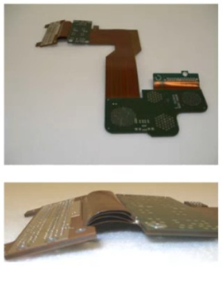
Figure 1: Bookbinder Rigid-Flex boards stack multiple Flex PCBs at a bend to easily fold open and close along a specific axis. Multiple bends at different parts of a construction facilitate bends at multiple axes with dual-axis and dual-bend configurations. Source: APCB
The Flex and Rigid-Flex PCBs serve a range of applications such as military, aerospace, robotics, and consumer electronics due to their size and weight gains. However, PCB designers who typically work with rigid boards must know that these constructions come with a different set of design rules that should be studied before and during the design. This tutorial lists some of the common pitfalls when designing Flex and Rigid-Flex PCBs.
Stackup and materials overview
The stackup for Rigid and Rigid-Flex uses different materials to maximize flexibility. Flex and Rigid-Flex boards are built to MIL-P-50884 and IPC 6013. The IPC-2221 through IPC-2225 are a set of design guidelines that can be used as a reference, while the IPC 4202, 4203, and 4204 standards prescribe the flexible-based dielectrics, metal clad dielectrics, and cover and bonding materials used for these constructions. All boards are tested to IPC-A-600 Class 2 (sometimes Class 3) for acceptability and final inspection.
Stackup
As specified in IPC 6013, there are five types of Flex and Rigid-Flex boards.
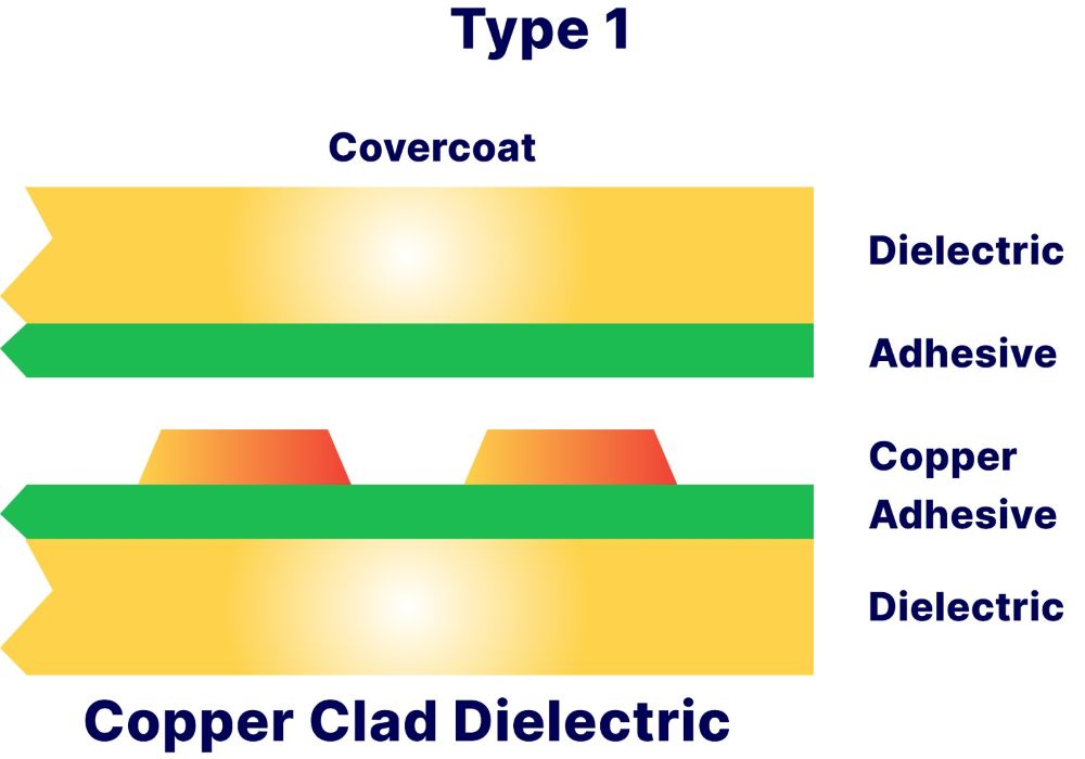
Type 1: Single-sided flexible printed boards containing one conductive layer, with or without stiffeners.
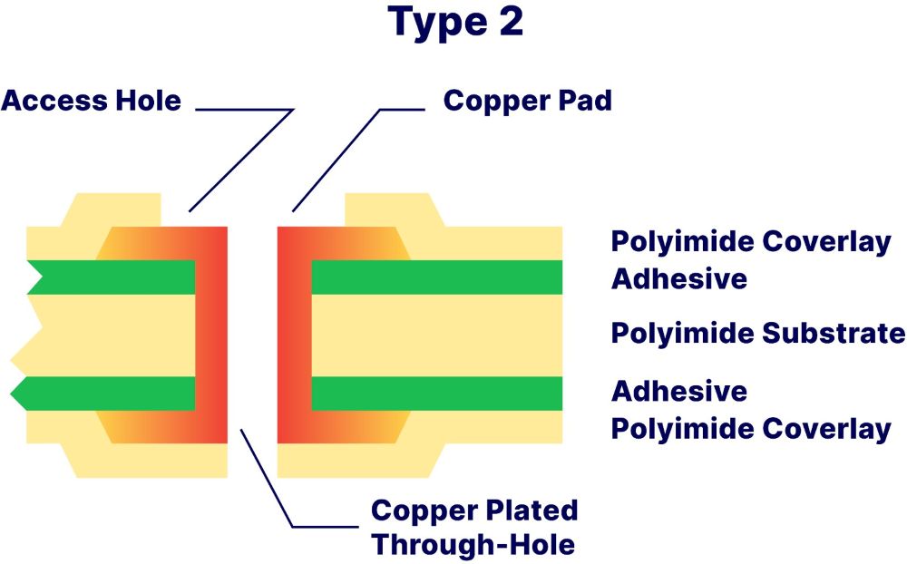
Type 2: Double-sided flexible printed boards containing two conductive layers with plated-through holes (PTHs), with or without stiffeners.
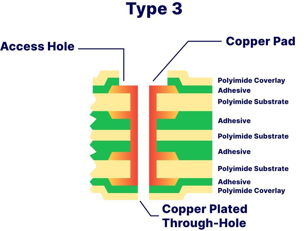
Type 3: Multilayer flexible printed boards containing three or more conductive layers with PTHs, with or without stiffeners.
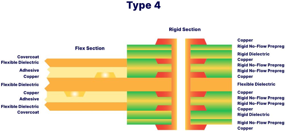
Type 4: Multilayer rigid and flexible material combinations containing three or more conductive layers with PTHs.
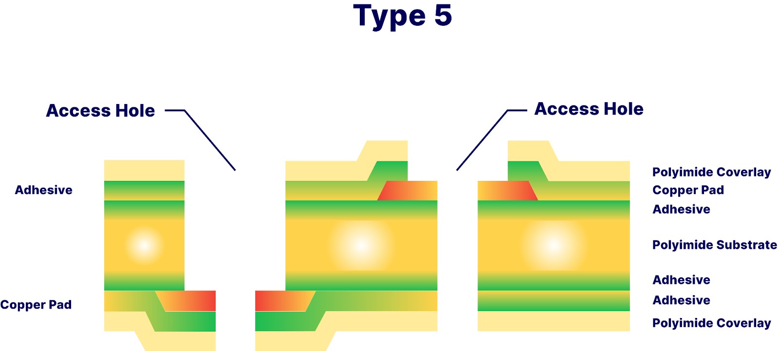
Type 5: Flexible or Rigid-Flex printed boards containing two or more conductive layers without PTHs.
Table 1 shows some Advanced PCB (APCB) Flex and Rigid-Flex specifications.
|
Specifications and tolerances |
|
|
Design guidelines |
IPC-2221 through IPC-2225 |
|
Built to |
IPC-A600, Class 2 (Class 3 when specified) |
|
Minimum lines and spaces |
2.5 mils (.0025”) |
|
Rigid-Flex layer count |
4 to 40 layers |
|
Flex layer count |
1 to 12 layers |
Table 1: APCB Flex and Rigid-Flex specifications.
Materials
Flex and Rigid-Flex boards include a covercoat or coverlay; base copper-clad material; bond ply and adhesive (or prepreg); and rigid laminates. A covercoat is a liquid photoimageable (LPI) material that serves the same function as the coverlay but does not require pre-routing. The base material can either be adhesive or adhesiveless. The coverlay is typically a polyimide film with an adhesive layer used to encapsulate and buffer the circuits on the outer layers. The coverlay material is pre-routed to match the surface features of the Flex PCB to ensure a precise coverage of the outer layers. Bond ply and adhesive materials hold the board together. For Flex boards, the bond ply is a polyimide film with an adhesive coating on both sides. For Rigid-Flex boards, no-flow prepreg is used.
Common pitfalls and best practices
Flex PCB basic calculations
Applications for flex circuits include static and dynamic movement along an axis. In a static application, the interconnect is bent or folded for installation and is bent minimally thereafter, e.g., during maintenance. The dynamic flexure requires intermittent to continuous bends, so flexible interconnects with carefully selected materials are needed. For example, this construction is used in armored vehicles to allow for the back door to drop for soldiers to climb in and out. The IPC 2223 defines the minimum bend radius as a multiplier of flex thickness. Materials such as thick copper and heavy adhesive may increase this number (Table 2).
|
Flex type |
Minimum bend radius |
|
Single-sided |
10x material thickness |
|
Double-sided |
20x material thickness |
Table 2: Minimum bend radius for single- and double-sided flex.
Designers may forget that the bend areas can stress component solder joints, leading to fatigue and failure. To avoid this, ensure there's enough distance between flex points and solder pads. Find other calculations and recommendations for Flex PCBs in Table 3.
|
Adhesive |
~1 mil per ounce of copper |
|
Back drill depth tolerance |
0.002” to 0.005” |
|
Covercoat opening |
.010 minimum per mil of adhesive over pad size |
Table 3: APCB Flex and Rigid-Flex recommended tolerances.
Manufacturing considerations
Blistering on the surface and delamination of the flex may occur if contaminants penetrate the PCB and trap unwanted moisture during manufacturing. To keep substances out of the flex area in foil constructions, create a pocket during processing. This is done by building the outer layers out of copper foil instead of copper-clad rigid dielectric. It is also important to consider the thickness of the copper traces when prerouting the coverlay material to ensure there are no air pockets when adhering to the surface of the PCB (Figure 2).
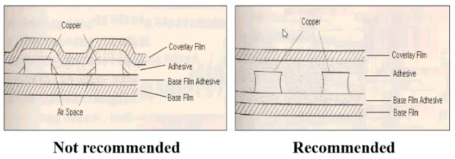
Figure 2: When using a coverlay, consider the thickness of the outer layer’s copper traces to ensure precise coverage of the PCB surface.
Source: APCB
Another manufacturing consideration is the need for a flexible epoxy “bead” at the rigid-to-flex junctions of a Rigid-Flex PCB. This “bead” prevents the no-flow prepreg of the rigid board from escaping onto the flex section. An overflow of the no-flow prepreg material creates a knife edge, cutting into the Flex PCB traces when bent. The “bead” has a tapered shape that creates a natural transition at this joint to help the flex layers bend more seamlessly (Figure 3).
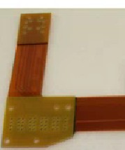
Figure 3: An epoxy “bead” is placed at the rigid-to-flex junctions to prevent the flow of the rigid board’s prepreg material from cutting into the Flex PCB. The “beads” shown in this image are the dark black lines at the junction points.
Source: APCB
Rounding out the edges
When starting the design for Rigid-Flex boards, you must keep the flexure in mind. This means that right angles and straight edges are best avoided in certain areas. For instance, avoid right angles in the routed part and use radius corners instead. Traces and circuit patterns should be more rounded. You can see some of these concepts in Figure 4 with pad connections, connections between pad land and traces, as well as establishing circuit patterns between areas with high pad land density and connected traces.
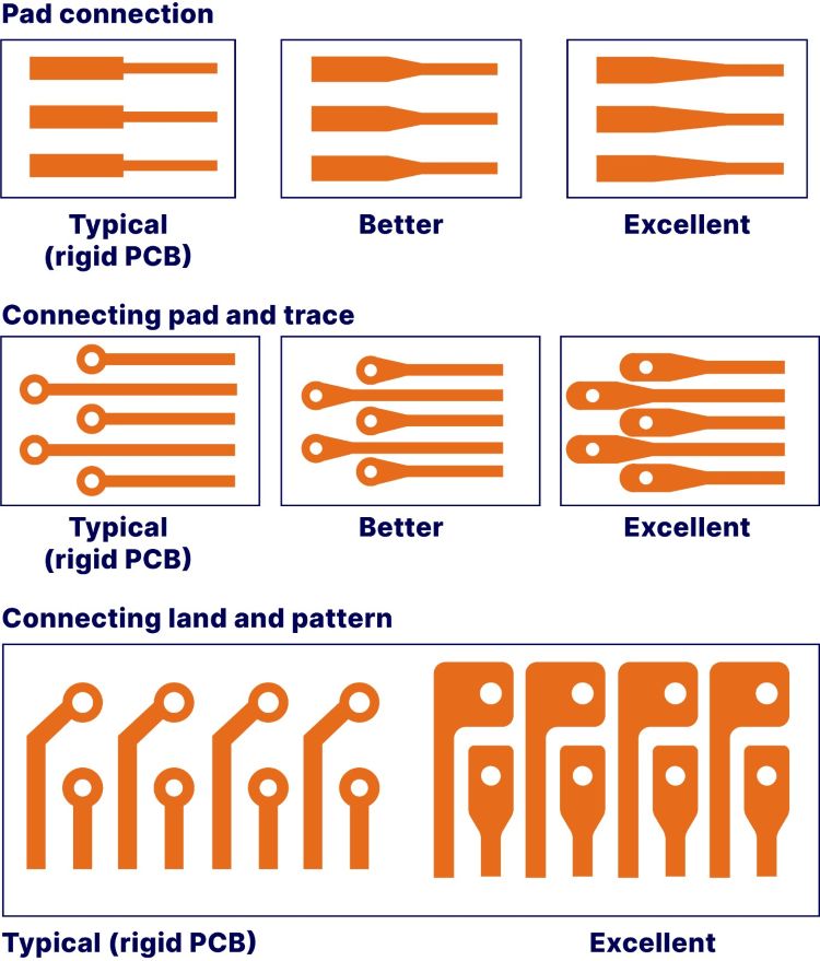
Figure 4: Flex PCBs require you to smooth out the “sharp” angles to avoid the intersecting lines and sharp points found in Rigid PCB traces. Note: considering the coverlay’s resin flow during the lamination phase of the board, the solder pad area has also increased to improve adhesion.
Source: APCB
Flex area considerations
It is critical to notice how the traces are routed. The flex area of Rigid-Flex and flex constructions comes with their own design and layout considerations in order to minimize stress to the components, solder joints, and the transitions between the Rigid and Flex boards.
Route all circuitry perpendicular to the bend across the flex area. This ensures that all traces experience the same mechanical strain across a bend. At the flex-to-rigid transitions, route traces take a 45o bend once inside the rigid section. The 45o angle should not be sharp, but rather a curved path that the trace takes back onto the rigid section. This is further highlighted in Figure 5.
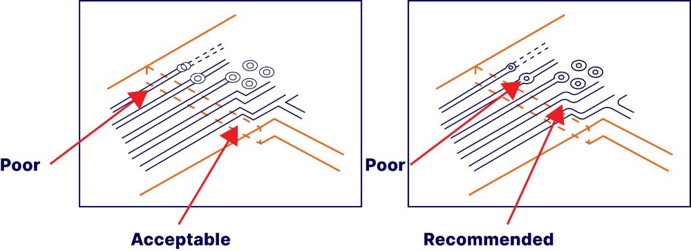
Figure 5: Recommended trace routing transitioning from a Flex PCB section onto a rigid section.
Source: APCB
Furthermore, do not crowd these rigid-to-flex junctions and bend areas with PTHs and vias. Any features should lay at least 100 mils away from these junctions to prevent undue stress.
For double-sided Flex PCBs with a high circuit density, you must understand how the mechanical stresses of a bend impact the circuit traces between flex layers. An overlap between traces in adjacent layers can create the “I-beam” effect, which makes the structure stronger, but far less flexible, causing failures with bending (Figure 6).

Figure 6: Stacking traces can lead to the “I-beam” effect making the board far less flexible.
Source: APCB
Conclusion
You must consider many aspects of your circuit well before designing the prototype due to design, layout, and manufacturing considerations. This tutorial covers a few of the most common pitfalls for Flex and Rigid-Flex PCB designs, but not all of them. Contact us to learn more about APCB’s Flex and Rigid-Flex capabilities.

AdvancedPCB
Related Posts

Fiducials in PCB Manufacturing: Design Rules, IPC Guidance, and Best Practices

Prototype PCB vs. Full Spec Production: A Guide for Design Engineers


