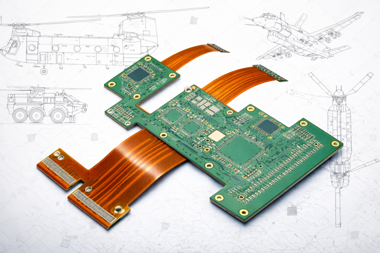
Gold fingers are the exposed, hard gold–plated edge connectors on printed circuit boards that slide into mating slots to create a reliable electrical interface. They are specifically designed for applications that require repeated insertion cycles, stable electrical performance, and long service life. Common in backplanes, daughtercards, and modular systems, gold fingers remain the preferred solution when durability and signal integrity matter.
This article explains what gold fingers are, how they are manufactured, and why they are used, with guidance to help engineers confidently specify a PCB with this feature.
What Are Gold Fingers?
Gold fingers are plated contact pads located along the edge of a PCB that function as plug-in connectors. Unlike standard surface finishes intended for soldering, gold fingers are engineered for sliding contact. Their primary role is to maintain low, consistent contact resistance through thousands of mating cycles while resisting wear, oxidation, and corrosion.
Gold fingers typically use hard electrolytic gold plated over a nickel barrier layer. The nickel acts as a diffusion barrier and provides mechanical strength, while the hard gold surface resists abrasion and fretting corrosion far better than tin or soft gold finishes. This construction keeps electrical performance stable over time, even in serviceable or hot-swap applications.
A controlled edge bevel is equally important. Beveling reduces insertion force, prevents damage to the mating connector, and improves alignment during insertion. For this reason, gold finger PCB designs typically specify tight tolerances for bevel angle, edge straightness, and coplanarity.
How Gold Fingers Are Manufactured
Gold finger fabrication follows standard PCB processing up to the point where additional steps are introduced for edge connector durability.
Design begins with defining finger length, pitch, spacing, keep-out zones, and bevel geometry, often with bevel angles between 20 and 45 degrees. These parameters should be reviewed early with the fabricator to ensure manufacturability.
After copper circuitry is fabricated, solder mask is applied while leaving the gold finger area fully exposed. The PCB edge is then beveled using controlled machining to achieve smooth insertion. Nickel is plated first, typically 3 to 7 microns thick, followed by hard electrolytic gold, commonly around 0.5 to 1.0 microns or more depending on required mating cycle life. This hard gold finish is fundamentally different from ENIG and is specifically intended for wear resistance rather than solderability.
Quality control includes XRF measurement of plating thickness, visual inspection for porosity or nodules, verification of bevel geometry, and cleanliness checks. Contamination on the contact surface can increase contact resistance and compromise long-term reliability.
Why Use Gold Fingers?
Gold fingers provide superior wear resistance and stable electrical performance compared to tin-plated contacts or separate board-to-board connectors. They support high mating cycle counts, reduce the risk of intermittent failures, and eliminate the need for additional connector hardware at the board edge.
From a signal integrity perspective, hard gold over nickel provides a smooth, consistent contact interface. When combined with controlled-impedance routing to the edge connector, this helps minimize reflections and insertion loss in high-speed interfaces.
Although hard gold plating increases initial fabrication cost, it often lowers total lifecycle cost by reducing maintenance, connector replacement, and field failures in modular and serviceable systems.
Relevant IPC Standards
Gold finger PCBs are commonly specified and evaluated using the following IPC standards:
-
IPC-6012 – Qualification and performance specification for rigid printed boards
-
IPC-A-600 – Acceptability of printed boards
-
IPC-2221 – Generic standard on printed board design
These standards define expectations for plating quality, visual acceptance, and mechanical integrity, while many applications also include custom requirements for gold thickness and mating durability.
_________________________________________________________________________________________
Frequently Asked Questions
What is the difference between hard gold and ENIG on PCBs?
Hard gold is electrolytically plated over a nickel barrier and is designed for wear resistance in sliding or repeated-mating contacts such as gold fingers. ENIG (electroless nickel immersion gold) is intended for solderability, not mechanical wear, and will degrade quickly if used in edge connector applications.
How thick should gold plating be on PCB gold fingers?
Gold thickness typically ranges from 0.5 to 1.0 microns or more, depending on the required number of mating cycles and reliability expectations. Higher cycle applications often specify thicker hard gold plating, which should be confirmed with the fabricator during design.
Why is beveling required on gold fingers?
Beveling reduces insertion force, improves alignment during mating, and minimizes wear on both the PCB and the connector. A properly controlled bevel helps prevent damage to the gold plating and ensures consistent electrical contact throughout the life of the product.


.png?resizemode=force&maxsidesize=1226)
