


Moving From Prototypes to Large-Scale Production

A challenge many electronics companies face is quickly moving from concept to product. No matter the application, you must quickly take your project through the design/ redesign, prototype, and scale lifecycle . You can see the Advanced PCB (APCB) cycle for this process in Figure 1.

Figure 1: APCB’s solution for building prototypes and pre-production production ramps to high-volume production and redesign. This process utilizes both domestic and global facilities.
While most organizations have the internal capability to move from concept to schematic capture and layout, ensuring a PCB is fully manufacturable at scale presents a different set of challenges. Design decisions that function in a prototype environment do not always translate cleanly into repeatable, high-volume production.
As programs transition beyond prototype, supplier selection becomes critical. APCB provides the technical depth, manufacturing legacy, and global infrastructure to support this progression. Domestic facilities handle both standard and advanced builds, while qualified offshore partners enable scalable, cost-efficient volume production. This structure allows customers to move rapidly from design validation to production release, with controlled process transfer and consistent quality across regions.
This tutorial outlines how APCB supports the path from quick-turn prototype through mass production.
Building a Prototype
PCB prototyping typically progresses through three phases: design, fabrication, and assembly. Many projects begin as redesigns rather than clean-sheet layouts, driven by performance optimization, miniaturization, compliance updates, or cost reduction.
Circuit design generates two foundational outputs that govern downstream execution:
- Board artwork (Gerber, ODB++, IPC-2581)
- Assembly documentation (BOM, pick-and-place, fabrication notes)
Layout is a critical point in manufacturability and long-term scalability. Component placement, stackup selection, trace geometry, and material choices directly affect impedance control, signal integrity, EMI/EMC performance, and thermal reliability.
Advanced designs may require:
- HDI architectures with blind, buried, or stacked microvias
- Controlled impedance structures for high-speed digital interfaces
- Rigid-Flex or Flex constructions for mechanical integration
- Stackup optimization to balance electrical performance and cost
While many OEMs maintain internal layout capability, APCB supplements these efforts through its engineering teams staffed with IPC-certified designers. This support reduces risk early in the lifecycle and improves downstream fabrication yield.
APCB converts validated designs into production-ready hardware with tightly controlled processes and repeatable execution. Six manufacturing facilities support prototype builds across a wide technology spectrum, including:
- Standard rigid multilayer with plated through-holes
- HDI constructions with blind, buried, and stacked vias
- Flex and Rigid-Flex architectures
Domestic and offshore sites operate under aligned quality systems to ensure design intent is preserved from prototype through production scale-up. This continuity minimizes respins, stabilizes yields, and enables predictable ramp-to-volume performance.Below is a map of APCB’s domestic and offshore manufacturing sites.

You can see the capabilities of the USA-based manufacturing facilities in Table 1. The domestic abilities are robust and provide the benefit of accelerated production cycles. APCB can offer quick-turn boards as soon as the next day for standard multi-layer (4-6 layer) rigid boards. For more complex boards, there are still quick-turn schedules, but they require increased communication with the designer and the front-end engineering of the specific APCB facility that focuses on that board type (e.g., HDI, Flex, Rigid-Flex).

Table 1: APCB’s 6 domestic manufacturing sites and their respective capabilities.
Assembly
The second output of the design is the data related to the assembly. This grants users the bill of materials (BOM), which lists the components used as well as their locations on the board.
Moving Toward Large-Scale Production
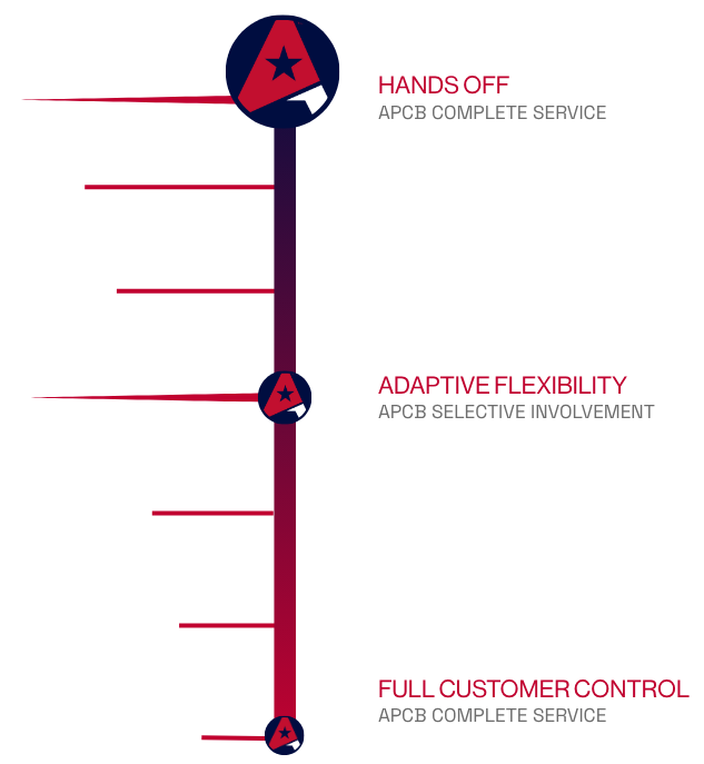
After the final design has been verified and is seen as a viable product, a business must scale to production. APCB offers a route to larger-scale offshore production with a spectrum of support. You can assume full control of all offshore manufacturing with APCB helping when needed, you can “hand off” to APCB allowing them to complete the service, or you can choose somewhere in the middle with selective involvement from APCB (Figure 3).
.png "Service-Levels-(2).png")
Figure 3: APCB’s global program solutions allow you to choose the level of support and control that you would like to have over offshore production.
Global Supply Chain Risks
A primary focus of technology companies is to innovate and deliver cutting-edge solutions fast. The list of new technologies is abundant, and so are the demands. It can be difficult for these companies, especially new businesses, to pivot their focus to introduce the right teams that can assess the technical, support, and logistical details of a global supply chain. Table 2 presents several risks that come with implementing a supply chain.
| Risk | Potential Consequence |
| Manufacturing lower-end technology in a higher-end facility | Incurring unnecessary costs |
| Manufacturing higher-end technology in a lower-end facility | Low production yield |
| Going with a broker or manufacturer that does not specialize in your product area and does not do an upfront intake profile to understand your needs | Production issues if the company cannot qualify and/or visit offshore manufacturing facilities frequently |
| Insufficient communication between the engineering staff that created the product prototype and the volume production engineering team | Potential defects in a whole production run, allowing competitors to have an advantage |
| Insufficient communication between the engineering staff that created the product prototype and the volume production engineering team | Lower production yield and slower time to market (TTM) |
| Working without inventory management | Difficulty turning a product into an off-the-shelf commodity, leading to longer lead times |
| The supplier cannot deliver during transportation disruptions | Product is not delivered in time anytime there are service disruptions. This delay becomes more significant when having to clear customs for international shipments. |
Table 2: A few potential risks and consequences that come with having a global supply chain.
Risk Mitigation with AdvancedPCB
AdvancedPCB is an experienced supplier that addresses supply chain risks head-on. With many pre-qualified and approved facilities to choose from, both domestic and offshore, we can match the technology to the factory to maximize customer yield by obtaining the best solution at the lowest cost.
Our manufacturing, engineering, and full-service staff oversee all production in offshore facilities. Products from offshore facilities that are involved with volume production are shipped back to our domestic facilities for inspection and compliance review. If any defects or concerns appear in this process, AdvancedPCB's domestic facilities will assume the rest of the volume manufacturing to ensure the PCB is fabricated according to industry standards. Furthermore, all our offshore facilities undergo a qualification process and maintain their own UL and ISO certifications, with several achieving TS, AS, or medical certifications.
AdvancedPCB also has flexible stocking programs (Figure 4) that allow customers to warehouse products in APCB’s distribution center or achieve custom stocking solutions. Inventory management programs are supported for “just in time” assemblies on custom PCBs. Finally, we are an experienced supplier that has pre-existing, dependable relationships with multiple carriers, allowing for more transportation options if one mode of transport is not available.

Summary
To keep up the pace with advancements, modern technology companies must be able to realize their design concept from the circuit, layout, first-run fabrication, and working prototype, all the way to pre-production ramp-ups and high-scale production. To do this successfully, it is important to work with an experienced PCB manufacturer who has comprehensive solutions with extensive engineering, manufacturing, production, and transportation expertise. APCB has the legacy and established facilities that can readily assist companies in building a product from the ground up. APCB offshore facilities welcome on-site or virtual audits with on-site program managers in Asia, and has a global team that is readily available to help. For more information visit https://www.advancedpcb.com/en-us/services/global-services/.
Related Posts

Prototype PCB vs. Full Spec Production: A Guide for Design Engineers

PCB Design for Data Centers: Enhancing Efficiency and Performance
