Understanding the CAM normalization process and how to avoid CAM holds
.png?resizemode=force&maxsidesize=500)
The CAM normalization process
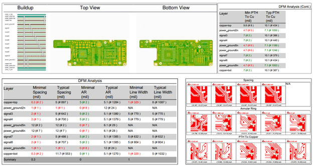
Computer-aided manufacturing (CAM) is the native software used by a manufacturer to automate and control its PCB fabrication equipment, such as laser direct imaging (LDI), drilling machines, lamination machines, and chemical baths. A required step, CAM normalization involves importing a customer’s design files into the manufacturer’s native software, which combs those files and makes adjustments so that the software can control AdvancedPCB’s equipment seamlessly (Figure 1).
Figure 1: Advanced PCB’s DFM engineers work directly with a customer’s PCB designs to ensure the design can be manufactured without issue.
The steps are as follows:- Rename customer files to AdvancedPCB’s standard naming convention.
- Ensure that all necessary files are present.
- Import Gerber and NC drill files into our CAM system.
- Review that the boards’ specifications in the order match the data supplied.
- Prepare the files for custom spec orders.
A basic review involves adjusting all aspects of the customer files to the standard naming convention and ensuring that all files are present. Then, the customer files (Gerber and NC drill files) can be imported into the CAM system. As Step 4 above shows, the board’s specifications must match the data supplied. Compare the Gerber files to non-Gerber prints and other documents. Non-standard, or custom specification, orders require basic modifications that are made to most sets of files received and will not alter the design in any way.
What is a CAM hold?
A CAM hold occurs when discrepancies are found within the customer’s PCB design files that will prevent the manufacturer from getting the board produced. These include:
Discrepancies between the board specifications in the Gerber files and the order.
Missing files from the customer’s order (aperture list, Excellon drill file, tool list, Geber files).
Errors from netlist comparisons (insufficient annular ring, insufficient copper trace. width/spacing, insufficient inner clearances, undersized soldermask clearances).
The DFM process
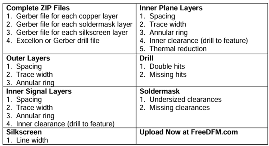
CAM holds can occur during CAM normalization or design for manufacturing (DFM), a process that ensures that the design is manufacturable. Some manufacturers offer software that lets customers check whether their design can be fabricated with the manufacturer’s in-house capabilities, or whether their board would meet the design requirements without EMI/RFI, EMC, or signal integrity issues. Advanced PCB offers a FreeDFM tool to check imported Gerber files and email the customer with the results.
Figure 2 lists the checks that the FreeDFM tool performs in the PCB out layers, inner plane layers, inner signal layers, solder mask, silkscreen, and drill files. If the tool is not used, you can find the manufacturing tolerances here.

Figure 2: The potential issues that FreeDFM can uncover.
The most common mistakes that lead to CAM hold
Missing filesAccording to our engineers, the most common issue is missing files. An order that comes in may not include everything:
- Gerber files
- Tool list
- Drill file
- Aperture list
- A full fabrication print required for custom spec orders exceeding $2k
Dimension conflicts
Pay close attention to the tolerances that your manufacturer specifies. The FreeDFM tool is designed to free the PCB designer from the task of tracking all dimensional details of the design. One major issue is dimension conflicts. These can arise for many reasons; typically, the board or array dimensions in the fabrication drawings may not match those in the Gerber files.
Without the tool, another common CAM hold occurs when designers create drill hits that are too small or too close to other small drill hits. Note that AdvancedPCB’s default hole tolerance is ±0.005" for holes up to .250”. Advanced PCB also offers a ±0.003" hole tolerance with a couple of prerequisites.
Figure 3 shows a potential CAM hold with an insufficient annular ring, which is the ring that surrounds the via. An insufficient annular ring, or a ring that is too thin, will not allow for complete plating on the via. This can also prevent proper hole placement, making it more difficult to center the drill on the via. AdvancedPCB requires a minimum .005" annular ring for vias or a minimum .007" for component holes for manufacturing.

Figure 3: Three views of an insufficient annular ring.
Another dimensional issue includes an insufficient copper trace width and trace spacing. Please see Table 1 for more detail on AdvancedPCB’s tolerances for the minimum trace width and spacing for 1 oz, 2 oz, 3 oz, and 4 oz boards.
| Copper weight | Inner or inner+outer layers | Minimum trace width | Minimum trace space |
| 1 oz | Finished copper weight (inner layers) | 0.003" | 0.003" |
| 2 oz | Finished copper weight (inner & outer) | 0.005" | 0.005" |
| 3 oz | Finished copper weight (inner & outer) | 0.009" | 0.009" |
| 4 oz | Finished copper weight (inner & outer) | 0.010" | 0.010" |
Gold finger issues
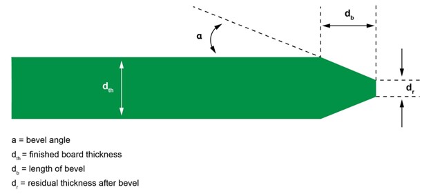
The use of gold fingers (or edge fingers), often found in card-edge PCB connections, come with limitations based on the specific manufacturer that the customer has chosen. Our gold fingers are beveled in accordance with Table 2, where Figure 4 shows the beveling that is accomplished by this process (𝛼 is the bevel angle, dth is the finished board thickness, db is the length of bevel, and dr is the residual thickness after the bevel).
They are gold-plated to increase conductivity and, thus, the integrity of the electrical connection. Please note that a thicker gold plating yields a connector edge with more mating cycles. It is also important to note that the remaining thickness left on the board after the bevel, or dr, depends on the finished thickness of the board (dth); therefore, this should be considered before choosing a more severe bevel angle, such as 20o. Standard AdvancedPCB board thicknesses are 20 mil, 31 mil, 62 mil, 93 mil, and 125 mil. The equation for the dr can be found below:
dr=dth-2dbsin(α)
| Standard or custom | Board thickness (dth) | Bevel angle (𝛼) | Length of bevel (db) | Residual thickness after bevel (dr) |
| Standard | .062” | 30o | .030” | .032” |
| Custom option | .062” | 45o | .025” | .027” |
| Custom option | .062” | 20o | .071” | .013” |

Figure 4: Bevels used to create gold fingers, where Advanced PCB does a standard 30o bevel or 45o or 20o options.
Board routing and panelization
Cutouts, non-plated slots, plate-through slots, internal routing, and milling channel specifying cutouts (internal routing) can lead to issues if these are not designed according to the manufacturer’s tolerances. Many designs will also have a missing board rout outline.
A tab route can be used to create arrays. However, tabs require 0.100" between individual boards for tab rout spacing. If APCB is meant to set up the array for the customer, a number of files are required as well as detailed information:
- The single board files (1-up files)
- The total number of boards in the array, e.g., 5 boards in X-direction, 10 boards in Y-direction
- The width of the top, bottom, left, and right rails (standard is 0.5")
- A drawing with the array configuration that is desired, including tooling holes, fiducials, and step and repeat requirements (if CAD data is sent as a 1-up image)
Finally, exposed copper may be viewable on the board edge, inside cutouts, or on non-plated drills. Routing a PCB contour can, for example, leave the copper traces exposed at the PCB edge. This is generally not preferred because it could make contact with neighboring conductors. The exposed copper will also eventually oxidize, which is a problem that could precipitate board failure in the field.
Leveraging CAM engineers is a necessary step in realizing a PCB design, because many new designers may not be familiar with “bringing a PCB to life.” The FreeDFM helps by finding and automatically fixing many potential CAM holds. Other issues that the tool finds will be brought to the designer’s attention well before the files are sent to the manufacturer. However, several issues can still crop up that would cause a CAM hold and prevent the PCB from being manufactured. Consider some of these common issues before submitting a design with a strict timeline.


