


Understanding High Density Interconnect PCBs for Precision Design
.png?resizemode=force&maxsidesize=500)
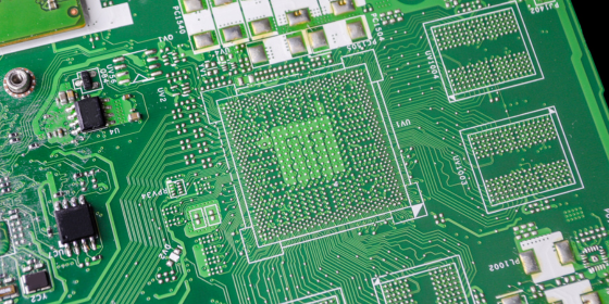
High density interconnect (HDI) PCBs use extremely concentrated routing interconnection coupled with a high component density. These PCBs accommodate key components such as BGAs with extremely small pitches and high pin counts that support a large range of I/Os. In turn, high-speed PCB signal lines support the I/Os. Microvias are utilized in HDI due to their reduction in signal path length, which improves signal integrity (SI) and shrinks size to maximize space. HDIs are sought out for space-constrained applications such as portable devices and wearables (Figure 1). This tutorial discusses HDI basics, illuminates potential design missteps when approaching HDI PCBs, and highlights AdvancedPCB’s (APCB’s) fabrication capabilities.
.png "PCB-Design-(1).png")
Figure 1: HDI is used to accommodate components with high-density pin counts and small pitches.
An overview of HDI
|
IPC-2226 |
Sectional Design Standard for HDI Printed Boards |
|
IPC/JPCA-2315 |
Design Guide for HDI and Microvia |
|
IPC/JPCA-4104 |
Specification for HDI and Microvia Materials |
|
IPC-6016 |
Qualification and Performance Specification for HDI Layers or Boards |
Table 1: IPC specifications for HDI.
HDI PCBs leverage blind, buried, stacked microvias, and via in pad (VIP) along with thinner trace widths to achieve a highly dense board. Using small blind vias in place of through-hole (TH) vias offers more reliability — according to the IPC — due to the greatly reduced aspect ratios (depth-to-width).
Naturally, the tightly packed traces and dense routing can lead to crosstalk and other SI issues in critical nets. Addressing these issues is critical before fabrication through various means, such as employing the right materials in the PCB stackup.
HDI boards are fabricated with a sequential build-up (SBU), expanding thin individual dielectric layers around a thick core (See Figure 3 for a sample buildup). The process follows similar steps to a standard multilayer board, using the photoresist coat and exposed deposition, and the subsequent develop/etch/strip step. Mechanical via formation using a drill or through laser drilling can be applied, where laser drilling offers much smaller vias for finer BGA pitches. Via metallization, meanwhile, is accomplished with direct metallization or electroless copper plating. At its core, HDI fabrication’s main element is the build with multiple lamination cycles before the final outer layer development.
HDI vias and routing considerations
BGA components ultimately determine the via size that the designer must employ. APCB’s manufacturing processes support micro BGA pitches of 0.2 mm with later drilled microvias. HDI routing is dependent upon the component pin density/pitches, component count/placement, chosen stackup, and via architecture. Tracking uniformity and minimum line width is critically important, as it must be considered to avoid open and short circuit conditions. Via placement considerations also include the distribution of blind and buried holes. An asymmetric stack design can result in uneven pressure, causing board warpage.
Routing considerations will change with HDI. For example, the microvia aspect ratio will often force a thinner substrate in the HDI’s outer layers, thus changing the dimensions of the controlled impedance (50-ohm single-ended or differential pair) transmission lines on the surface layers. Many designers, for this reason, will bury transmission lines within the internal layers for a wider trace width.
HDI routing can be tricky given the density, particularly when considering BGA fanout. For the BGA’s outer rows, you can choose to directly fan out. When considering a BGA’s inner rows, designers often must drop signals down a layer and fan out to escape the device perimeter. This widens the available trace width, since traces do not have to be squeezed between the BGA pads. Microvias are either stacked or staggered to support this fanout, as shown in Figure 2.

Figure 2: Effective design will take advantage of HDI benefits in stacking microvias instead of staggering them to connect traces to the outer, second, and third rows of a BGA package.
Via in pad (VIP) offers distinct HDI design advantages. Instead of routing a via to an arbitrary point on the PCB with a trace, the via is built directly on the component’s pad — allowing designers to directly access inner layers from the component’s pin. Microvia-in-pad designs are typically laser ablated and full copper filled. However, these designs can also be mechanically drilled and filled with conductive or non-conductive materials. High pin count BGAs that run hot might benefit from the use of conductive VIP epoxies to maximize heat dissipation.
Component layout and ground rules
The high density of HDI PCBs calls for designers to pay close attention to component placement — ensuring viability in soldering, installation, and maintaining boards. Planning ahead and allowing the maximum space tolerances while still taking advantage of the available density facilitates any necessary future reworking. It is important to not place vias under any chip unless done for thermal relief. Doing so prevents solder from wicking through the vias and remaining under the chip, potentially creating short circuits. VIP should be copper-capped while the opposite side should either be copper-capped or covered by a solder mask, ensuring that plating chemicals do not get trapped within the via.
HDI Materials
HDI boards are prone to unique manufacturing constraints where the selected materials will impact both electrical performance and manufacturing cost. As stated previously, HDI PCBs will use advanced, generally thinner laminates than materials used in conventional PCBs such as FR4. High speed and high frequency signal considerations will involve using materials with a stable dielectric constant (DK) and low dissipation factor (Df), where special low-loss epoxy formulations are often used to strike a balance between cost/manufacturability and performance. These materials have a high glass transition temperature (Tg), ensuring they are rigid and stable structures with a strong dimensional stability. As a result, there are minimal changes in electrical length at varying temperatures — a critical aspect of maintaining a stable impedance of a transmission line or differential pair. APCB offers a wide range of materials options from vendors such as 3M, Arlon, Bergquist, Isola, Rogers, ITEQ, Taconic, Ventec and more. For more information on APCB’s laminates, please read “Choosing the right laminate material for your PCB design.”
ELIC
The Every Layer Inter-Connection (ELIC) technique is popular in smartphone design, as it offers smaller pitches and the elimination of space-consuming mechanical holes inside the board. The process uses layers of copper-filled stack microvia-in-pads so that designers can make connections between any two PCB layers. Figure 3 shows a cross-sectional view of a 14-layer ELIC stackup with 6 lamination cycles (6 lam) done by APCB.
.png "PCB-Stackup-(4).png")
Figure 3: Stackup of a HDI PCB with 6 lam ELIC with 14 layers and the vendors of each lamination layer.
APCB fabrication capabilities
APCB facilities house state-of-the-art equipment to build out HDI PCBs, with features such as microvias (stacked and staggered), blind vias, buried vias, and VIP. We support micro BGA pitches as low as 0.2 mm through our laser drilling capabilities, which allow us to achieve precise depth control. Laser direct imaging (LDI) capabilities ensure exacting registration and that all multilayer inner cores receive a thorough check using Automated Optical Inspection (AOI) units for excellent defect detection. Manufacturing supports HDI buildup with as many at 7x lam cycles, with support for up to 42 layer boards and .00275” trace/space. Table 2 shows the capabilities of various APCB facilities.

Table 2: HDI capabilities of various APCB facilities.
A list containing some of APCB’s HDI tolerances/capabilities can be seen in Table 3.

Table 2: APCB’s advanced technology capabilities to support HDI.
HDI PCBs come with their own unique design considerations, ranging from component placement and routing to via architecture and build-up. This board density ensures that engineers must carefully consider material selection and areas where SI may degrade. Within the same size PCB, HDI technology accommodates more connections with a lower layer count than traditional PCBs, making them highly useful for small form factor solutions. Leveraging advanced in-house capabilities, APCB can support designers with their HDI fabrications.
Related Posts

2-Layer vs. 4-Layer Printed Circuit Boards: How to Choose the Right Option
.png?resizemode=force&maxsidesize=1226)
AdvancedPCB Expands HDI Capability in Silicon Valley with Advanced Vacuum Via Filling Technology
