


4-Layer vs. 6-Layer PCB: When to Add Layers

Choosing between a 4-layer and a 6-layer printed circuit board (PCB) is an important design decision that affects electrical performance, routing flexibility, manufacturability, and cost. While adding layers can provide more routing space and improve the ability to manage signal integrity, electromagnetic interference (EMI), and power distribution, a higher layer count does not automatically produce a better PCB.
When should you choose a 6-layer PCB instead of a 4-layer PCB? A 4-layer PCB is often sufficient when routing density is manageable, power distribution is straightforward, and signals can maintain continuous reference paths. A 6-layer PCB becomes advantageous when additional routing space, ground reference planes, improved power distribution, or separation of sensitive circuits is needed. The decision should be based on electrical requirements, stackup design, manufacturability, and total production cost—not data rate alone.
Understanding the differences between these two multilayer constructions helps engineers select a PCB stackup that supports both design performance and efficient manufacturing.
What Is the Difference Between a 4-Layer and 6-Layer PCB?
A multilayer PCB consists of alternating conductive copper layers and insulating dielectric materials laminated together into a single structure. Copper layers provide pathways for electrical signals, power distribution, and grounding, while dielectric materials electrically isolate the conductive layers.
A 4-layer PCB contains four conductive copper layers. A common configuration uses two outer signal layers, one internal ground plane, and one internal power plane. This construction provides more routing flexibility and better reference-plane control than a typical 2-layer PCB while remaining relatively economical to manufacture.
A 6-layer PCB contains six conductive copper layers. The two additional layers create more options for signal routing, ground references, and power distribution. Depending on the stackup, engineers can allocate additional layers to signal routing or continuous reference planes to address more demanding electrical requirements.
Both constructions can support controlled impedance, high-speed signals, and complex component layouts. The difference is the flexibility available to organize those electrical functions within the board.
4-Layer vs. 6-Layer PCB Comparison
| Design Considerations | 4-Layer PCB | 6-Layer PCB |
|---|---|---|
| Copper layers | 4 | 6 |
| Fabrication cost | Generally lower | Generally higher |
| Routing flexibility | Fewer available routing layers | More options for routing and plane allocation |
| Ground planes | Often one dedicated ground plane | Can accommodate multiple ground planes |
| Power distribution | Internal planes, coppper pours, and traces | More flexibility for dedicated power distribution |
| Controlled impedance | Supported with appropriate stackup design | Supported with addtitional stackup design |
| EMI performance | Effective with proper grounding and layout | Potential for improved EMI control through plane placement |
| Board thickness | Configurable | Configurable |
| Via structures | Through-hole and optional HDI structures | Through-hole and optional HDI structures |
| Typical applications | Microcontroller boards, industrial controls, and moderate-density electronics | High-density digital designs, mixed signal systems, and complex power distribution |
How PCB Layer Count Affects Signal Integrity and EMI
Signal integrity becomes increasingly important as digital edge rates increase, routing distances grow, and circuit density rises. Fast transitions contain high-frequency energy even when the underlying signal's data rate or clock frequency is relatively low. PCB layer count influences the designer's ability to control impedance, provide consistent signal references, and manage electromagnetic coupling between circuits.
Return-Path Control and Ground Planes
Every electrical signal requires a return-current path to complete its circuit. For high-frequency signals, return current tends to concentrate near the signal conductor on an adjacent reference plane, where the electromagnetic fields are closely coupled. A continuous reference plane helps reduce current-loop area, control impedance, and limit unwanted electromagnetic emissions.
On a 4-layer PCB, designers commonly use an internal ground plane to provide a reference for signals routed on the adjacent outer layer. However, depending on the stackup, signals on the opposite outer layer may reference a power plane instead.
A 6-layer PCB provides more flexibility to position continuous ground planes near critical signal layers. This can simplify return-path management and reduce the need to route sensitive signals across changes in reference planes.
Design consideration: Avoid routing critical high-speed signals across splits or gaps in their reference planes. When signals transition between layers, evaluate how the return current transfers between reference conductors. Ground stitching vias or appropriately placed decoupling capacitors may be needed, depending on the reference-plane arrangement.
Controlled Impedance
Controlled impedance is essential for many high-speed digital, RF, and communication interfaces. A trace's characteristic impedance depends on several factors, including:
- Trace width and copper thickness
- Dielectric thickness between the trace and its reference plane
- Dielectric constant (Dk) of the PCB material
- Trace geometry and spacing from nearby conductors
- Whether the trace uses microstrip or stripline construction
Both 4-layer and 6-layer PCBs can support controlled-impedance routing.
The advantage of six layers is greater flexibility to position signal layers relative to reference planes and select dielectric thicknesses that support the required impedance. For example, a 6-layer design may provide additional opportunities to route critical signals internally while reserving outer layers for component connections and less-sensitive routing. However, adding layers does not inherently allow wider traces for a given impedance. Trace geometry must be calculated using the actual material properties and finished stackup dimensions.
Engineers should work with their PCB manufacturer to establish the stackup and impedance requirements before finalizing controlled-impedance trace widths.
Crosstalk and Electromagnetic Interference
Crosstalk occurs when electromagnetic energy from one conductor couples into another nearby conductor. Its severity depends on factors such as trace spacing, parallel routing length, reference-plane geometry, signal characteristics, and the dielectric environment. Additional PCB layers can help engineers separate sensitive signals from noisy circuits and allocate routing space more effectively.
A well-designed 6-layer stackup may also position signal layers between continuous reference planes, helping contain electromagnetic fields. When signal layers are adjacent without a separating reference plane, routing traces in different directions can help reduce broadside coupling. However, orthogonal routing alone does not eliminate crosstalk.
For EMI-sensitive designs, continuous reference planes, controlled return paths, appropriate component placement, and proper decoupling remain critical regardless of layer count.
Power Distribution and Thermal Considerations
Layer count also affects how power reaches components and how heat moves through the PCB.
Power Distribution Network Design
The power distribution network (PDN) delivers regulated voltages to integrated circuits and other electrical loads while maintaining acceptable voltage stability. Modern processors, FPGAs, and other digital devices can draw rapidly changing currents, creating demands on the PDN.
A low-impedance PDN typically combines:
- Power and ground planes or copper regions
- Decoupling capacitors placed near component power connections
- Short, low-inductance connections between capacitors and power pins
- Appropriate via placement and conductor dimensions
- Voltage regulation designed for the expected load and transient response
A 4-layer PCB can provide effective power distribution when the number of supply rails and circuit density are manageable. A 6-layer PCB offers more flexibility to dedicate copper layers or regions to power distribution while maintaining reference planes for critical signals. Closely spaced power and ground planes can also provide distributed capacitance, although this effect depends on plane area, dielectric thickness, and material properties. It does not replace the need for appropriate discrete decoupling capacitors.
When does an additional layer help? If power routing consumes substantial space on signal layers, multiple voltage rails are difficult to distribute, or reference-plane continuity is being compromised, a 6-layer construction may provide a more effective solution.
Thermal Management
Copper conducts heat more effectively than typical PCB dielectric materials, making copper planes and conductive pathways useful for spreading thermal energy away from heat-generating components. Additional copper layers may improve heat distribution when they are properly connected to thermal pads, vias, and other heat-transfer structures. However, increasing layer count does not automatically reduce component temperatures.
Thermal performance depends on the amount and location of copper, copper thickness, thermal via design, component placement, board materials, airflow, and available heat-transfer paths. For power-dense designs, engineers should evaluate whether additional layers provide meaningful thermal benefits or whether improvements such as heavier copper, thermal vias, larger copper areas, or external heatsinking would be more effective.
IPC-2152 provides guidance on conductor current-carrying capacity and temperature rise. Although it is useful for evaluating conductor heating, comprehensive thermal management may also require simulation and application-specific testing.
Common 4-Layer and 6-Layer PCB Stackups
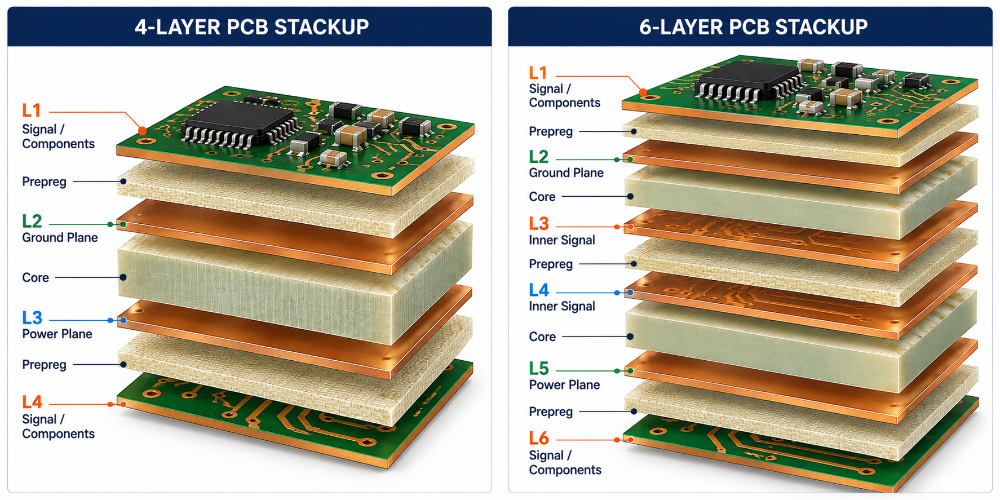
A PCB stackup defines the sequence of conductive and dielectric layers within a multilayer board. The stackup affects impedance, signal referencing, power distribution, board thickness, mechanical stability, and manufacturing requirements. The following examples illustrate possible constructions. They are starting points rather than universal recommendations.
Typical 4-Layer PCB Stackup
| Layer | Function |
|---|---|
| L1 | Top Signal / Components |
| L2 | Ground Plane |
| L3 | Power Plane |
| L4 | Bottom Signal / Components |
In this configuration, signals routed on L1 can reference the adjacent L2 ground plane. Signals on L4 may reference the L3 power plane, depending on the routing geometry and dielectric spacing. This arrangement can work well when the power plane provides an appropriate reference and the return-current paths are properly managed. However, fragmented power planes or multiple isolated voltage regions can complicate high-speed routing on L4.
For designs with more demanding signal-integrity requirements, engineers may consider alternative 4-layer arrangements that prioritize continuous ground references.
Key design consideration: The distance between each signal layer and its reference plane influences impedance and electromagnetic coupling. A nominally symmetrical stackup does not guarantee equivalent signal performance on both outer layers.
In this configuration, signals routed on L1 can reference the adjacent L2 ground plane. Signals on L4 may reference the L3 power plane, depending on the routing geometry and dielectric spacing. This arrangement can work well when the power plane provides an appropriate reference and the return-current paths are properly managed. However, fragmented power planes or multiple isolated voltage regions can complicate high-speed routing on L4.
For designs with more demanding signal-integrity requirements, engineers may consider alternative 4-layer arrangements that prioritize continuous ground references.
Key design consideration: The distance between each signal layer and its reference plane influences impedance and electromagnetic coupling. A nominally symmetrical stackup does not guarantee equivalent signal performance on both outer layers.
Typical 6-Layer PCB Stackup
| Layer | Function |
|---|---|
| L1 | Top Signal / Components |
| L2 | Ground Plane |
| L3 | Inner Signale |
| L4 | Power Plane |
| L5 | Ground Plane |
| L6 | Bottom SIgnal / Components |
This configuration provides two dedicated ground planes and additional routing capacity. L1 can reference L2, while L6 can reference L5. The L3 signal layer lies between L2 and L4, so its electrical performance depends on the continuity and geometry of both reference planes. If L4 contains split power regions, special attention is needed when routing signals on L3.
An alternative six-layer construction may prioritize additional signal layers, different power-plane placement, or tightly coupled ground and power planes. No single six-layer arrangement is optimal for every application.
Important: The final stackup should be developed with the PCB manufacturer using the required finished thickness, dielectric materials, copper weights, impedance targets, and available core and prepreg constructions.
Why Stackup Symmetry Matters
Multilayer PCBs are generally designed with balanced constructions to reduce manufacturing distortion. Differences in copper distribution, dielectric thickness, and material properties can contribute to warpage during lamination and thermal processing. Balanced stackups help manage these effects, but copper distribution and material selection must also be considered.
A 6-layer PCB does not necessarily need to be thicker than a 4-layer PCB. Both can be manufactured to common nominal finished thicknesses when suitable materials and dielectric constructions are available.
When Should You Move from 4 Layers to 6 Layers?
The decision to add layers should be driven by identifiable design requirements rather than a general assumption that more layers improve performance.
When a 4-Layer PCB Is Sufficient
A 4-layer PCB may be the best choice when:
- Component density allows routing without excessive congestion.
- Critical signals have suitable continuous reference paths.
- Power distribution can be implemented without compromising signal routing.
- Controlled-impedance requirements can be met with the available stackup.
- EMI performance can be achieved through appropriate layout and grounding.
- Cost and manufacturing simplicity are important design priorities.
Many microcontroller-based systems, industrial controllers, sensor interfaces, and general-purpose electronic products can be implemented effectively using four layers.
Importantly, there is no universal data-rate threshold that determines whether a PCB requires six layers. Some high-speed interfaces can be routed successfully on four layers, while lower-speed systems with dense components or complex power requirements may benefit from six.
When a 6-Layer PCB Is Justified
A 6-layer PCB becomes worth considering when:
1. Routing density exceeds the available space. High-pin-count components, dense BGAs, and numerous interconnections may require additional routing channels.
2. Critical signals need better reference-plane continuity. Additional layers can provide more options for positioning ground planes near sensitive or high-speed routes.
3. Multiple voltage rails complicate power distribution. A six-layer construction may allow more dedicated copper area for power delivery without sacrificing signal-routing capacity.
4. EMI requirements are difficult to meet. Additional reference planes and routing flexibility can help reduce coupling and support more effective return-path management.
5. Mixed-signal circuits need better separation. Additional routing and plane options may simplify the physical organization of analog, digital, and power circuitry. Proper grounding and return-path design remain essential.
6. Fine-pitch components create routing congestion. More signal layers can help with fanout and escape routing, although some packages may still require HDI features such as microvias.
Before increasing layer count, engineers should also evaluate whether improved placement, more efficient routing, revised plane allocation, or changes to the component package could resolve the problem. Adding layers is one design option—not a substitute for sound layout practices.
Cost and Manufacturing Considerations
A 6-layer PCB generally costs more to manufacture than a comparable 4-layer PCB because it requires additional copper and dielectric materials, more innerlayer processing, and additional manufacturing inspection and handling. However, the cost difference depends on more than layer count. View our PCB manufacturing capabilities.
Lamination and Via Structures
Standard 4-layer and 6-layer PCBs using conventional plated through-hole vias can often be manufactured with a single final multilayer lamination cycle. Therefore, increasing from four to six layers does not automatically require additional sequential lamination cycles.
Manufacturing complexity increases when the design requires blind vias, buried vias, or microvias that must be formed and interconnected during additional processing stages. These structures can improve routing access and support high-density designs, but they also introduce additional fabrication requirements. Where component density allows, using conventional through-hole vias may help control the cost of a 6-layer PCB.
Material Selection and Finished Thickness
Additional layers require a different combination of copper foils, cores, and prepregs to achieve the specified finished board thickness. The PCB manufacturer must account for material availability, dielectric thickness, copper distribution, lamination behavior, and manufacturing tolerances. High-speed designs may also require specific laminate properties, including controlled dielectric constant and dissipation factor.
Selecting a material solely because it supports a higher layer count is not sufficient. The material must meet the electrical, thermal, mechanical, and reliability requirements of the application.
Via Reliability and Aspect Ratio
Plated through-hole reliability is influenced by board thickness, drilled-hole diameter, plating quality, material properties, and thermal exposure. The via aspect ratio is generally defined as the drilled-hole depth divided by the drilled-hole diameter. Higher aspect ratios can make plating more challenging and may affect manufacturing yield and reliability.
Although a 10:1 aspect ratio is sometimes used as a general design guideline, acceptable limits depend on the manufacturer's process capabilities and the applicable performance requirements.
Engineers should confirm drilled-hole dimensions, finished-hole requirements, and plating capabilities with the fabricator. Teardrops may improve conductor-to-pad connection robustness and manufacturing tolerance, but they are not a primary solution for plated-barrel fatigue caused by thermal cycling.
Total Cost of Ownership
The lowest fabrication price does not always produce the lowest overall product cost.
A 6-layer PCB may justify its additional cost if it:
- Reduces routing congestion and design iterations.
- Helps achieve signal-integrity or EMI requirements.
- Simplifies power distribution.
- Avoids more expensive HDI structures.
- Reduces the risk of redesign after testing.
For high-volume products, even a modest per-board cost difference can be significant. For prototype and development programs, the value of reducing engineering time and design risk may outweigh the additional fabrication cost.
The best decision considers both manufacturing cost and the engineering consequences of the selected layer count.
IPC Standards for 4-Layer and 6-Layer PCB Design
Several IPC standards provide guidance for designing and manufacturing reliable multilayer PCBs. While no IPC standard dictates whether a design requires four or six layers, the following are relevant to stackup selection, materials, and manufacturing quality.
- IPC-2221 and IPC-2222: Establish general and rigid-board-specific design requirements, including conductor spacing, multilayer construction, and interconnections.
- IPC-4101: Defines specifications for laminate and prepreg materials, including dielectric properties, thermal performance, and dimensional stability.
- IPC-6012: Establishes qualification and performance requirements for rigid PCBs, including plated-hole integrity and structural requirements for applicable performance classes.
- IPC-A-600: Provides visual acceptability criteria for manufactured PCBs, including conductor features, registration, and plated-hole conditions.
- IPC-2141 and IPC-2152: Provide guidance on controlled impedance and conductor current-carrying capacity, respectively. IPC-2141 is a legacy reference and should be supplemented with modern impedance modeling.
- IPC-TM-650: Contains test methods for evaluating PCB materials and manufactured board characteristics.
Engineers should specify applicable IPC standards, revisions, performance classes, and testing requirements in their fabrication documentation. Layer count alone does not determine IPC compliance or PCB reliability. View all quality assurance certifications >
How AdvancedPCB Supports Multilayer PCB Manufacturing
Choosing between four and six layers is most effective when PCB designers and manufacturing engineers collaborate before the layout is finalized. AdvancedPCB supports multilayer PCB manufacturing with engineering expertise and design-for-manufacturability (DFM) guidance to help customers align electrical requirements with practical fabrication capabilities.
Our teams can help evaluate factors such as:
- Multilayer stackup construction and material selection
- Controlled-impedance requirements
- Dielectric thickness and copper weight
- Trace, space, and annular ring requirements
- Via structures and drilled-hole capabilities
- Finished board thickness and manufacturing tolerances
- Fabrication complexity, cost, and lead time
AdvancedPCB also supports quick-turn prototyping and production requirements across its U.S. manufacturing operations, with available capabilities and turnaround times dependent on the selected facility and project specifications. Engaging with the PCB manufacturer early can help identify potential fabrication constraints, avoid unnecessary complexity, and reduce the likelihood of design revisions.
Planning a 4-layer or 6-layer PCB? Contact AdvancedPCB to discuss your stackup, material, and manufacturing requirements before finalizing your design.
.png)
AdvancedPCB
Related Posts

The Benefits of Multilayer PCBs
