


PCB Stackup Resources
Choosing the right PCB stackup is one of the most consequential decisions in any design. The stackup dictates how many layers the board has, how those layers are arranged, and which materials bind them together. These choices steer signal integrity, electromagnetic compatibility, thermal behavior, manufacturability, and cost. Below are practical PCB stackup resources and examples to help you plan, document, and build with confidence.
What a PCB Stackup Is and Why Does It Matter?
A PCB stackup is the ordered structure of copper conductors and insulating dielectrics. Typical copper layers include:
- Signal layers for routing traces
- Plane layers providing solid copper for ground or power
- Mixed layers that combine routing with copper pours
Dielectric layers come in two main types: core (a fully cured laminate with copper on both sides) and prepreg (partially cured resin-glass sheets that bond layers during lamination).
The stackup defines impedance and propagation delay for high-speed nets, impacting timing and jitter. Reference planes and well-managed return paths cut EMI and crosstalk. Dielectric thickness and copper weight influence heat spreading and current capacity. Layer count and material selection determine yield, reliability, and price.
Common Stackups
Standard layer arrangements provide reliable starting points when building or selecting pcb stackups:
- Two-layer: Two layers are sufficient for simple, low-speed, or cost-constrained designs with careful return path management. Top and bottom signal with ground pours. Useful for basic MCU boards, modest power converters, and compact sensor modules. Keep high-speed traces short, pour continuous ground where possible, and add stitching vias for return paths.
- Four-layer: Four layers add internal planes that improve power distribution and EMI performance for most digital and mixed-signal products. Signal 1 / Ground / Power / Signal 2 is a practical baseline. It supports controlled-impedance microstrip on outer layers with a solid ground reference, easing decoupling and improving EMI for mid-speed digital and mixed-signal designs.
- Six-layer: Six or more layers are recommended for dense BGAs, controlled-impedance routing, and high-speed interfaces that benefit from dedicated planes and stripline channels. Common options include S1 / GND / S2 (stripline) / S3 (stripline) / PWR / S4, or S1 / GND / S2 / S3 / PWR / S4, depending on routing needs. With solid ground and power planes plus inner striplines, these stacks deliver tighter impedance control and isolation for high-speed buses, dense BGAs, and low-noise analog.
Standard PCB: Multi-layer Stackup
Typical PCB stackups for specified layer count and finished thickness for 1 oz copper layer* | ||||
|---|---|---|---|---|
4-layer | 6-layer | 8-layer | 10-layer | |
0.020" | 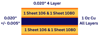.png) | |||
0.031" | 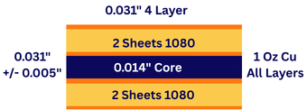.png) | 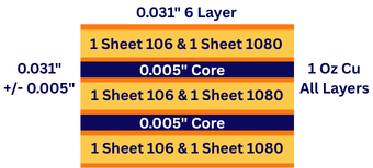.png) | ||
0.062" | 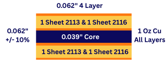.png) | 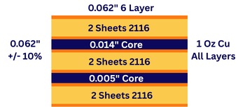.png) | 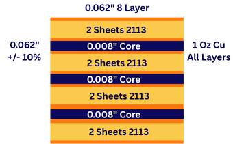.png) | 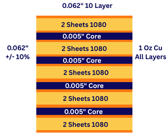.png) |
0.093" | 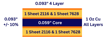.png) | 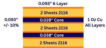.png) | 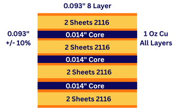.png) | 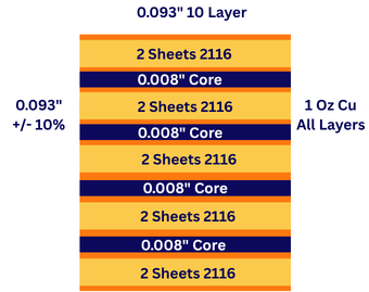.png) |
0.125" | 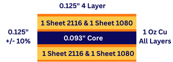.png) | 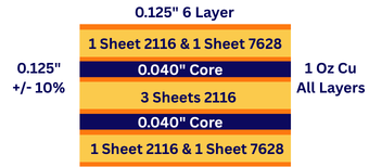.png) | 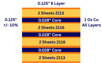.png) | 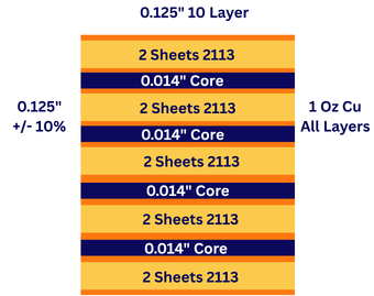.png) |
Max board size | 16" x 22" | 16” x 22” | 16” x 22” | 14” x 20" |
*These printed circuit board stackups are not "Guaranteed" unless you so specify in your Gerber files used when placing your printed circuit board order.
Advanced PCBs: Multi-layer Stackups
For these or any specific stackup that you require, be sure to order as "Custom" and select "Controlled Dielectric". You may select ½, 1 or 2 ounce inner layer copper foil for your printed circuit board.
Calculate the thickness of your custom stackup.
The chart that we link to below provides the thickness for a single ply (sheet) of each style of Pre-Preg after processing. These are grouped by the weight and type of the internal conductor layer (typical signal and plane layers) that they will be adjacent to (columns A-F). Those that are adjacent to the top and bottom copper layers will use the column designated for these (column G) regardless of the layer type. All plies that are not directly against a conductor layer (use for situations with more than 2 plies in an opening) will use the additional plies values (column H). These values are based on a minimum of 2 plies of pre-preg per opening between foil and cores or between cores.
| Thickness guide (mils, 1/1000 inch)*,** | ||||||||
|---|---|---|---|---|---|---|---|---|
| A | B | C | D | E | F | G | H | |
| Pre-Preg Styles | Against core with .5 oz copper and signal traces utilizing 30% of the board area | Against core with .5 oz copper and signal traces utilizing 70% of the board area | Against core with 1 oz copper and signal traces utilizing 30% of the board area | Against core with 1 oz copper and signal traces utilizing 70% of the board area | Against core with 2 oz copper and signal traces utilizing 30% of the board area | Against core with 2 oz copper and signal traces utilizing 70% of the board area | Against the top and bottom copper layers (foil) | Additional plies that are not directly against conductor layers |
| 106 | 1.9 | 2.2 | 1.5 | 2.0 | 0.5 | 1.5 | 2.3 | 2.1 |
| 1080 | 2.6 | 2.8 | 2.1 | 2.6 | 1.1 | 2.2 | 3.0 | 2.7 |
| 2113 | 3.5 | 3.7 | 3.0 | 3.5 | 2.0 | 3.1 | 3.9 | 3.5 |
| 2116 | 4.7 | 4.9 | 4.2 | 4.7 | 3.2 | 4.3 | 5.1 | 4.6 |
| 7628 | 6.5 | 6.8 | 6.0 | 6.5 | 5.0 | 6.1 | 6.9 | 6.2 |
*This thickness guide is provided as a guide only. The actual thickness will be affected by the copper distribution within the design as well as within the production panels
**The dielectric thickness requirements supplied with an order will be interpreted with a minimum, 10% tolerance.
Example:
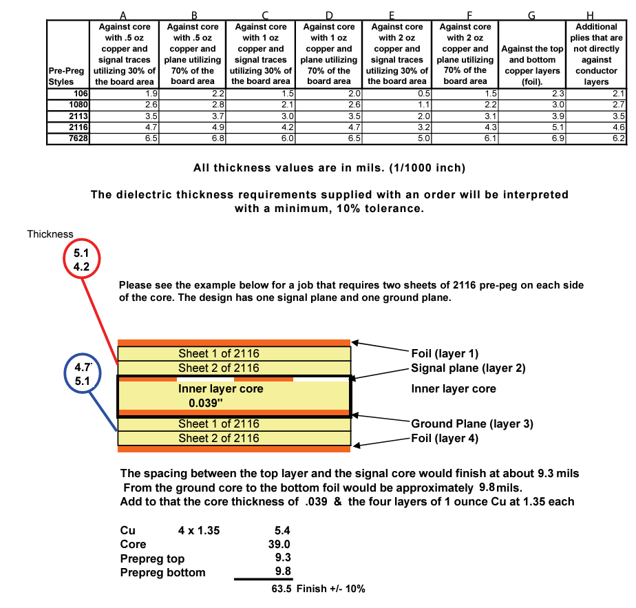
| Layer | Layer Description | Thickness |
|---|---|---|
| Layer 1 | Foil: 1 oz foil thickness 0.00135” | 0.00135” |
| Prepreg top | Sheet 1 of Prepreg style 2116 (Column G, Row 2116: 5.1 mils) | 0.0051” |
| Prepreg top | Sheet 2 of Prepreg style 2116 (Column C, Row 2116: 4.2 mils) | 0.0042” |
| Layer 2 | Signal Plane: 1 oz foil thickness 0.00135” | 0.00135” |
| Core | Laminate core 0.039” | 0.039” |
| Layer 3 | Ground Plane: 1 oz foil thickness 0.00135” | 0.00135” |
| Prepreg bottom | Sheet 1 of Prepreg style 2116 (Column D, Row 2116: 4.7 mils)) | 0.0047” |
| Prepreg bottom | Sheet 2 of Prepreg style 2116 (Column G, Row 2116: 5.1 mils) | 0.0051” |
| Layer 4 | Foil: 1 oz foil thickness 0.00135” | 0.00135” |
| Total thickness (Finish +/- 10%) | 0.0635” | |
See the following table for the final thickness options of our multilayer boards:
| 0.020" | 0.031" | 0.040" | 0.047" | 0.062" | 0.093" | 0.125" | Max Board Size | |
|---|---|---|---|---|---|---|---|---|
| 4-Layer | ✔ | ✔ | ✔ | ✔ | ✔ | ✔ | ✔ | 16" x 22" |
| 6-Layer | X | ✔ | ✔ | ✔ | ✔ | ✔ | ✔ | 16" x 22" |
| 8-Layer | X | X | X | X | ✔ | ✔ | ✔ | 16" x 22" |
| 10-Layer | X | X | X | X | ✔ | ✔ | ✔ | 14" x 20" |
| 11-Layer and Up | X | X | X | X | ✔ | ✔ | ✔ | >14" x 20" |
Tools, Documentation, and Manufacturing Readiness
Clear stackup documentation accelerates quoting and fabrication and reduces risk. Provide:
- A layer stack table from top to bottom with layer names, copper weights, materials, and target dielectric thicknesses
- A materials list with laminate and prepreg part numbers, glass styles, Dk/Df values at your design frequency, and applicable ratings
- Per-layer thickness tolerances and total board thickness
- Controlled-impedance notes specifying targets, tolerance bands, test method, and coupon requirements
Design-for-manufacturability considerations:
- Plan panelization to suit board thickness, copper balance, and tab strength
- Select via types (through, blind/buried, microvia) supported at your thickness and layer count
- Maintain adequate annular rings based on drill and registration tolerances
- Confirm minimum trace/space by copper weight and etch process
- Balance copper across layers to minimize bow and twist, particularly in thin or high-layer-count builds
AdvancedPCB’s engineering team can review your proposed pcb stackup, run impedance checks, and verify manufacturability prior to release.
What to include in your fabrication package:
- Stackup drawing and controlled-impedance callouts
- Drill tables with via types and any back-drilling notes
- Thermal requirements such as metal backing, copper coins, or heat spreaders
- Flex/rigid-flex bend area definitions, coverlay specs, adhesives, and stiffener details
Maintain a clear link between the layers in PCB documentation and the material callouts so that your pcb layer stackup can be reproduced consistently from prototype through production.