How Printed Circuit Boards Are Assembled: The Complete PCB Assembly Process
Posted
7/8/2026
How Printed Circuit Boards Are Assembled: The Complete PCB Assembly Process
A fabricated PCB is just a carrier — copper traces, drilled holes, and a solder mask, but no way to do anything on its own. PCB assembly (often shortened to PCBA) is the process that turns that bare board into a functioning electronic product: mounting components, soldering them in place, and verifying every connection actually works. Fabrication builds the roads; assembly puts the cars on them.
The two stages are handled by different equipment and, often, different facilities. Fabrication produces the copper layers, drills the holes, and applies solder mask and silkscreen. Assembly picks up from there — placing components, either manually or with automated pick-and-place machines, and soldering them using reflow or wave soldering. Since the boards frequently move fab-to-assembly across facilities (or even companies), a clean handoff of files and data matters as much as the physical process itself.
Whether you're developing a new electronic product, selecting a manufacturing partner, or learning how circuit boards are built, understanding the PCB assembly process helps engineers make better design decisions and improve manufacturability. Knowing how components are placed, soldered, inspected, and tested can reduce production issues, improve product reliability, simplify troubleshooting, and accelerate the transition from prototype to full-scale production.
PCB Assembly Process at a Glance
Printed circuit board assembly (PCBA) transforms a bare PCB into a fully functional electronic assembly by mounting, soldering, inspecting, and testing electronic components. While the exact process varies depending on the product, component mix, production volume, and reliability requirements, most PCB assemblies follow the same core manufacturing workflow.
Before any board is loaded onto a line, DFA/DFM engineers review this package — checking component footprints against actual part dimensions, spacing between parts, drill-file alignment, thermal relief on pads, and edge clearance. Catching a problem here costs a design revision; catching it after assembly starts costs scrapped boards. This review also flags any incoming quality control (IQC) issues with sourced components before they reach the line.
The workmanship itself is measured against established standards: IPC-A-610 (acceptability criteria for solder joints, component placement, and overall workmanship), IPC-J-STD-001 (materials and methods for soldered assemblies), IPC-7711/7721 (rework and repair procedures), and ISO 9001 (general quality management). A shop citing these isn't just checking a compliance box — they define exactly what a “good enough” solder joint or placement looks like.
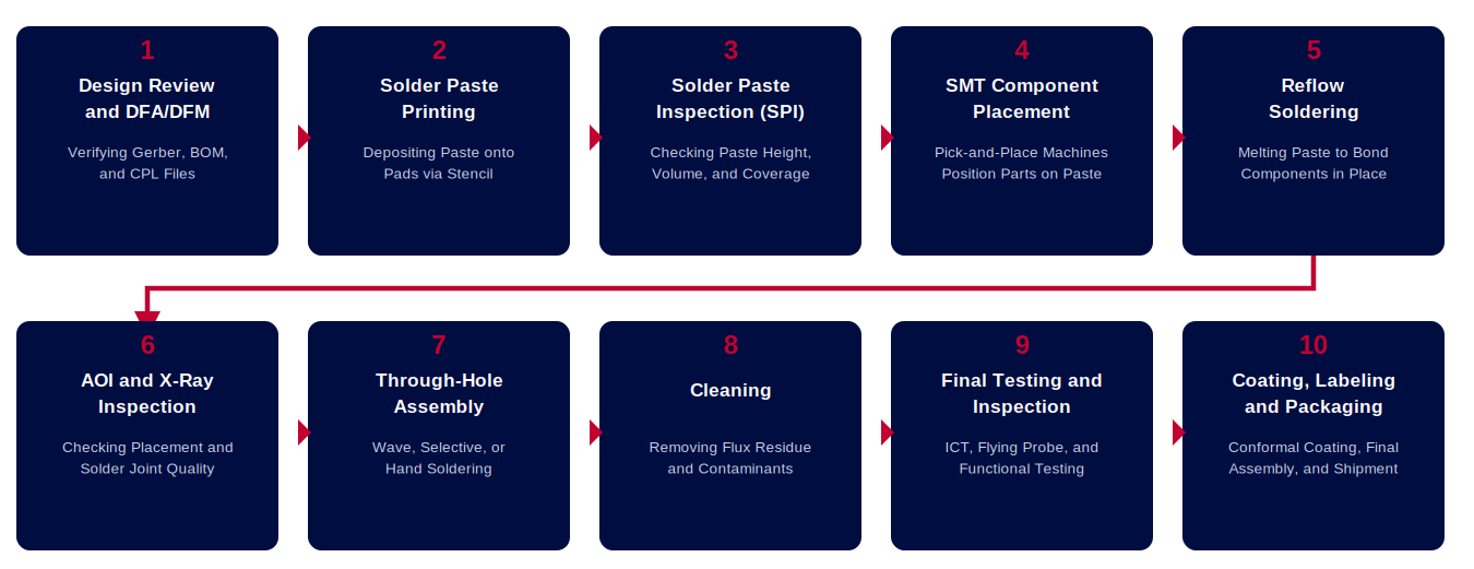
Below is the assembly process for a standard board carrying both surface-mount and through-hole components, start to finish.
Ten-step PCB assembly process flow from design review through packaging and shipment

Three-step solder paste stencil printing process: align, print, lift

Component placement and reflow soldering: pick-and-place followed by the reflow oven
Automated Optical Inspection (AOI) uses high-resolution cameras to compare the assembled board against a reference image, flagging missing components, wrong orientation, lifted leads, solder bridges, or insufficient solder. It's fast enough to check every board on a production line without slowing throughput.
X-ray inspection picks up where AOI's cameras can't see — specifically, solder joints hidden underneath a component body. Ball grid arrays (BGAs) and other leadless packages solder from underneath, so their joints are invisible to a camera but show up clearly on an X-ray, revealing voids, insufficient solder, or misalignment that would otherwise go undetected until the board failed in the field.
AOI, X-ray, and ICT/flying probe inspection methods used in PCB assembly
Three soldering methods cover THT assembly, and a single board may use more than one:
Wave soldering, selective soldering, and hand soldering compared side by side
Mixed-technology boards — carrying both SMT and THT parts — always run SMT first, since it depends on precise placement and reflow heat; through-hole components go on afterward and are soldered using whichever of the three methods fits.
Some components can't tolerate this wash cycle. These non-washable parts are set aside earlier in the process and soldered afterward, typically by hand, using no-clean flux that doesn't require a post-solder wash.
This step is skipped if using a no-clean process.
In-Circuit Testing (ICT) uses a bed-of-nails fixture, a grid of spring-loaded pins that contact predefined test points across the board simultaneously, to check for shorts, opens, and correct component values. It's fast and thorough but requires building a custom fixture, which makes sense for higher-volume runs and less sense for a one-off prototype.
Flying Probe Testing (FPT) achieves much the same result without a fixture: one or more probes move freely across the board's surface, contacting test points in sequence based on the design's netlist. It's slower per board than ICT but far more flexible, since there's no hardware to build or retool between design revisions, making it the natural choice for prototypes and lower-volume runs.
Functional testing goes a step further, powering the board and verifying it performs its intended function end-to-end, sometimes alongside burn-in testing for products with high reliability requirements.
Conformal coating applies a thin protective layer — acrylic, silicone, polyurethane, epoxy, or vapor-deposited parylene, depending on the required chemical and moisture resistance — over the finished assembly to guard against moisture, dust, and chemical exposure. Each material trades off differently between protection level, cost, and how easily the coating can be reworked later.
Shield cover assembly adds a metallic cover — aluminum, copper, or stainless steel — over sensitive areas of the board to block electromagnetic interference (EMI), both keeping outside EMI from disrupting the board and containing the board's own emissions so they don't interfere with neighboring devices. The cover is typically soldered, clipped, or adhered in place.

Finished solder joint cross section showing an SMT fillet, a through-hole lead, and conformal coating
From there, the board is integrated into its enclosure if applicable, labeled with serial numbers or traceability markings, and packaged — usually in anti-static, moisture-controlled materials — for shipment. At this point it has gone from a bare board to a finished, tested product.
PCB Assembly Process Summary
PCB assembly transforms a bare printed circuit board into a fully functional electronic assembly through a series of carefully controlled manufacturing processes. From design review and solder paste printing to automated component placement, soldering, inspection, testing, and final packaging, every step is designed to ensure the finished assembly meets the required electrical, mechanical, and quality standards. By understanding the complete PCB assembly process, engineers can improve manufacturability, reduce production issues, accelerate product development, and deliver reliable electronic products that perform as intended in the field.
How Printed Circuit Boards Are Assembled: The Complete PCB Assembly Process
A fabricated PCB is just a carrier — copper traces, drilled holes, and a solder mask, but no way to do anything on its own. PCB assembly (often shortened to PCBA) is the process that turns that bare board into a functioning electronic product: mounting components, soldering them in place, and verifying every connection actually works. Fabrication builds the roads; assembly puts the cars on them.
The two stages are handled by different equipment and, often, different facilities. Fabrication produces the copper layers, drills the holes, and applies solder mask and silkscreen. Assembly picks up from there — placing components, either manually or with automated pick-and-place machines, and soldering them using reflow or wave soldering. Since the boards frequently move fab-to-assembly across facilities (or even companies), a clean handoff of files and data matters as much as the physical process itself.
Whether you're developing a new electronic product, selecting a manufacturing partner, or learning how circuit boards are built, understanding the PCB assembly process helps engineers make better design decisions and improve manufacturability. Knowing how components are placed, soldered, inspected, and tested can reduce production issues, improve product reliability, simplify troubleshooting, and accelerate the transition from prototype to full-scale production.
PCB Assembly Process at a Glance
Printed circuit board assembly (PCBA) transforms a bare PCB into a fully functional electronic assembly by mounting, soldering, inspecting, and testing electronic components. While the exact process varies depending on the product, component mix, production volume, and reliability requirements, most PCB assemblies follow the same core manufacturing workflow.
Before any board is loaded onto a line, DFA/DFM engineers review this package — checking component footprints against actual part dimensions, spacing between parts, drill-file alignment, thermal relief on pads, and edge clearance. Catching a problem here costs a design revision; catching it after assembly starts costs scrapped boards. This review also flags any incoming quality control (IQC) issues with sourced components before they reach the line.
The workmanship itself is measured against established standards: IPC-A-610 (acceptability criteria for solder joints, component placement, and overall workmanship), IPC-J-STD-001 (materials and methods for soldered assemblies), IPC-7711/7721 (rework and repair procedures), and ISO 9001 (general quality management). A shop citing these isn't just checking a compliance box — they define exactly what a “good enough” solder joint or placement looks like.
Below is the assembly process for a standard board carrying both surface-mount and through-hole components, start to finish.

Ten-step PCB assembly process flow from design review through packaging and shipment

Three-step solder paste stencil printing process: align, print, lift

Component placement and reflow soldering: pick-and-place followed by the reflow oven
Automated Optical Inspection (AOI) uses high-resolution cameras to compare the assembled board against a reference image, flagging missing components, wrong orientation, lifted leads, solder bridges, or insufficient solder. It's fast enough to check every board on a production line without slowing throughput.
X-ray inspection picks up where AOI's cameras can't see — specifically, solder joints hidden underneath a component body. Ball grid arrays (BGAs) and other leadless packages solder from underneath, so their joints are invisible to a camera but show up clearly on an X-ray, revealing voids, insufficient solder, or misalignment that would otherwise go undetected until the board failed in the field.

AOI, X-ray, and ICT/flying probe inspection methods used in PCB assembly
Three soldering methods cover THT assembly, and a single board may use more than one:
Wave soldering, selective soldering, and hand soldering compared side by side
Mixed-technology boards — carrying both SMT and THT parts — always run SMT first, since it depends on precise placement and reflow heat; through-hole components go on afterward and are soldered using whichever of the three methods fits.
Some components can't tolerate this wash cycle. These non-washable parts are set aside earlier in the process and soldered afterward, typically by hand, using no-clean flux that doesn't require a post-solder wash.
This step is skipped if using a no-clean process.
In-Circuit Testing (ICT) uses a bed-of-nails fixture, a grid of spring-loaded pins that contact predefined test points across the board simultaneously, to check for shorts, opens, and correct component values. It's fast and thorough but requires building a custom fixture, which makes sense for higher-volume runs and less sense for a one-off prototype.
Flying Probe Testing (FPT) achieves much the same result without a fixture: one or more probes move freely across the board's surface, contacting test points in sequence based on the design's netlist. It's slower per board than ICT but far more flexible, since there's no hardware to build or retool between design revisions, making it the natural choice for prototypes and lower-volume runs.
Functional testing goes a step further, powering the board and verifying it performs its intended function end-to-end, sometimes alongside burn-in testing for products with high reliability requirements.
Conformal coating applies a thin protective layer — acrylic, silicone, polyurethane, epoxy, or vapor-deposited parylene, depending on the required chemical and moisture resistance — over the finished assembly to guard against moisture, dust, and chemical exposure. Each material trades off differently between protection level, cost, and how easily the coating can be reworked later.
Shield cover assembly adds a metallic cover — aluminum, copper, or stainless steel — over sensitive areas of the board to block electromagnetic interference (EMI), both keeping outside EMI from disrupting the board and containing the board's own emissions so they don't interfere with neighboring devices. The cover is typically soldered, clipped, or adhered in place.

Finished solder joint cross section showing an SMT fillet, a through-hole lead, and conformal coating
From there, the board is integrated into its enclosure if applicable, labeled with serial numbers or traceability markings, and packaged — usually in anti-static, moisture-controlled materials — for shipment. At this point it has gone from a bare board to a finished, tested product.
PCB Assembly Process Summary
PCB assembly transforms a bare printed circuit board into a fully functional electronic assembly through a series of carefully controlled manufacturing processes. From design review and solder paste printing to automated component placement, soldering, inspection, testing, and final packaging, every step is designed to ensure the finished assembly meets the required electrical, mechanical, and quality standards. By understanding the complete PCB assembly process, engineers can improve manufacturability, reduce production issues, accelerate product development, and deliver reliable electronic products that perform as intended in the field.
A fabricated PCB is just a carrier — copper traces, drilled holes, and a solder mask, but no way to do anything on its own. PCB assembly (often shortened to PCBA) is the process that turns that bare board into a functioning electronic product: mounting components, soldering them in place, and verifying every connection actually works. Fabrication builds the roads; assembly puts the cars on them.
The two stages are handled by different equipment and, often, different facilities. Fabrication produces the copper layers, drills the holes, and applies solder mask and silkscreen. Assembly picks up from there — placing components, either manually or with automated pick-and-place machines, and soldering them using reflow or wave soldering. Since the boards frequently move fab-to-assembly across facilities (or even companies), a clean handoff of files and data matters as much as the physical process itself.
Whether you're developing a new electronic product, selecting a manufacturing partner, or learning how circuit boards are built, understanding the PCB assembly process helps engineers make better design decisions and improve manufacturability. Knowing how components are placed, soldered, inspected, and tested can reduce production issues, improve product reliability, simplify troubleshooting, and accelerate the transition from prototype to full-scale production.
PCB Assembly Process at a Glance
Printed circuit board assembly (PCBA) transforms a bare PCB into a fully functional electronic assembly by mounting, soldering, inspecting, and testing electronic components. While the exact process varies depending on the product, component mix, production volume, and reliability requirements, most PCB assemblies follow the same core manufacturing workflow.
- Design Review and Manufacturing Data Preparation. Manufacturing files, the bill of materials (BOM), pick-and-place data, and assembly drawings are reviewed to verify design-for-manufacturability (DFM) and design-for-assembly (DFA) requirements before production begins.
- Solder Paste Printing. A precision stencil deposits controlled amounts of solder paste onto the PCB pads where surface-mount components will be installed.
- SMT Component Placement. Automated pick-and-place machines accurately position surface-mount components onto the solder paste deposits using vision-guided alignment.
- Reflow Soldering. The populated PCB passes through a controlled reflow oven where the solder paste melts and forms permanent electrical and mechanical connections.
- Inspection. Solder Paste Inspection (SPI), Automated Optical Inspection (AOI), and X-ray inspection verify solder quality, component placement, and hidden solder joints before assembly continues.
- Through-Hole Assembly. Through-hole components are installed and soldered using wave soldering, selective soldering, or hand soldering, depending on the design requirements.
- Cleaning. Flux residues and other contaminants are removed when required to improve long-term reliability and prepare the assembly for testing or conformal coating.
- Electrical Testing and Final Inspection. In-Circuit Testing (ICT), Flying Probe Testing (FPT), functional testing, and final visual inspection verify that the completed assembly meets electrical, mechanical, and quality requirements.
- Conformal Coating, Packaging, and Shipment. When specified, protective coatings, EMI shielding, labeling, and traceability markings are applied before the finished assemblies are packaged using ESD-safe materials and prepared for shipment.
Before Assembly Starts: Files, Standards, and Design Review
Assembly runs on data, not intuition. A complete assembly package includes Gerber or ODB++ files (board geometry), a bill of materials (BOM) listing every part with its manufacturer number and package type, pick-and-place (CPL/centroid) files giving the X/Y coordinates, rotation, and side for every component, NC drill files, and a solder paste stencil file. Miss one, and the risk is real: reversed polarity, missing parts, or components mounted in the wrong spot.Before any board is loaded onto a line, DFA/DFM engineers review this package — checking component footprints against actual part dimensions, spacing between parts, drill-file alignment, thermal relief on pads, and edge clearance. Catching a problem here costs a design revision; catching it after assembly starts costs scrapped boards. This review also flags any incoming quality control (IQC) issues with sourced components before they reach the line.
The workmanship itself is measured against established standards: IPC-A-610 (acceptability criteria for solder joints, component placement, and overall workmanship), IPC-J-STD-001 (materials and methods for soldered assemblies), IPC-7711/7721 (rework and repair procedures), and ISO 9001 (general quality management). A shop citing these isn't just checking a compliance box — they define exactly what a “good enough” solder joint or placement looks like.
Below is the assembly process for a standard board carrying both surface-mount and through-hole components, start to finish.
Ten-step PCB assembly process flow from design review through packaging and shipment
Surface Mount Technology (SMT) Assembly
Most modern boards are populated primarily with surface-mount components — parts soldered directly onto pads on the board surface rather than through drilled holes. SMT allows smaller, denser designs, supports components on both sides of the board, and is built for automation, which is why it dominates high-volume assembly.Solder paste printing
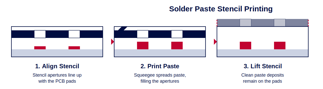
The process starts by depositing solder paste — a mixture of powdered metal solder and flux — onto the exposed copper pads. A thin stainless-steel stencil, laser-cut with an opening over every pad, sits directly on the board; a squeegee blade drags paste across the stencil, filling each aperture, and lifting the stencil leaves clean, precisely sized deposits behind.Three-step solder paste stencil printing process: align, print, lift
Solder paste inspection (SPI)
Before any components go on, automated SPI equipment checks the printed paste. 2D systems measure the height and width of each deposit; 3D systems add volume, giving a more complete picture. Either way, this step catches missing paste, insufficient volume, or bridging between pads before it becomes a soldering defect.Component placement
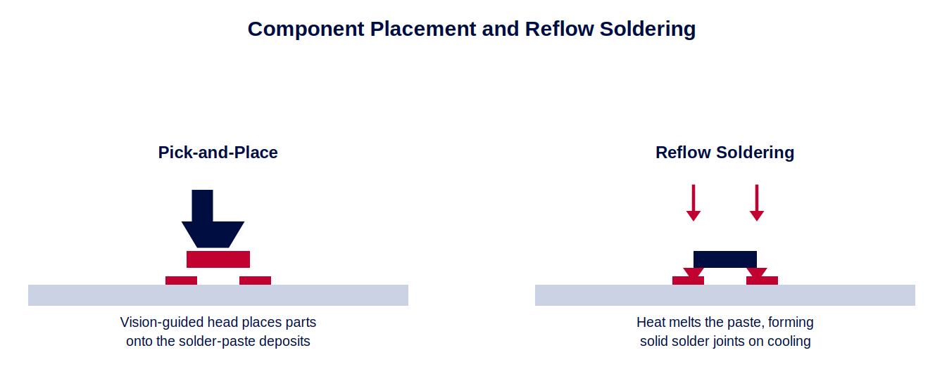
A pick-and-place machine takes over next, lifting components from tape, tube, or tray feeders, checking orientation and polarity with a built-in vision system, and setting each part onto its paste deposit. High-throughput lines place tens of thousands of components an hour, which is what makes dense, mixed-component boards economical to build at all.Reflow soldering
The populated board then travels through a reflow oven on a conveyor, following a controlled temperature profile that ramps up, melts the solder paste, and cools it back down. Peak temperatures depend on the paste: roughly 180–220°C for leaded solder, 210–250°C for lead-free. As the paste cools, it forms a solid metallurgical bond between each component lead and its pad.Component placement and reflow soldering: pick-and-place followed by the reflow oven
Inspecting the SMT Board
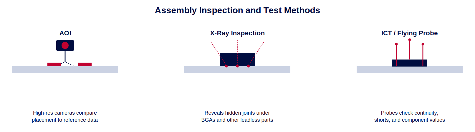
With components soldered, the board goes through inspection before anything else touches it.Automated Optical Inspection (AOI) uses high-resolution cameras to compare the assembled board against a reference image, flagging missing components, wrong orientation, lifted leads, solder bridges, or insufficient solder. It's fast enough to check every board on a production line without slowing throughput.
X-ray inspection picks up where AOI's cameras can't see — specifically, solder joints hidden underneath a component body. Ball grid arrays (BGAs) and other leadless packages solder from underneath, so their joints are invisible to a camera but show up clearly on an X-ray, revealing voids, insufficient solder, or misalignment that would otherwise go undetected until the board failed in the field.
AOI, X-ray, and ICT/flying probe inspection methods used in PCB assembly
Through-Hole Assembly
Some components — connectors, large capacitors, transformers — need more mechanical strength than a surface-mount pad can provide. These use through-hole technology (THT): leads pass through drilled holes and are soldered to pads on the opposite side, which handles physical stress and repeated connector insertion far better than a purely SMT joint.Three soldering methods cover THT assembly, and a single board may use more than one:
- Wave soldering passes the populated board over a standing wave of molten solder, soldering every through-hole lead on the underside in a single pass. It's the standard choice for boards with a meaningful number of THT parts.
- Selective soldering directs a nozzle to solder specific holes one at a time, using robotic positioning instead of a full wave. It's used when only a few THT components are present on an otherwise SMT-heavy board, or when nearby SMT parts can't tolerate the wave.
- Hand soldering covers components too sensitive, too large, or too oddly placed for automated methods, and is also the default for prototypes and very low volumes.
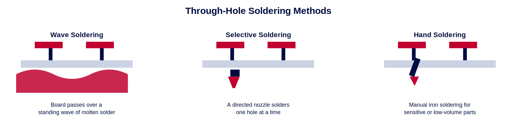
Wave soldering, selective soldering, and hand soldering compared side by side
Mixed-technology boards — carrying both SMT and THT parts — always run SMT first, since it depends on precise placement and reflow heat; through-hole components go on afterward and are soldered using whichever of the three methods fits.
Cleaning and Non-Washable Components
Once soldering is complete, the board is washed typically with deionized water jets, run at controlled temperature and pressure to remove flux residue and other contaminants left behind by soldering. Residue left on the board isn't just cosmetic: it can degrade electrical insulation and long-term reliability.Some components can't tolerate this wash cycle. These non-washable parts are set aside earlier in the process and soldered afterward, typically by hand, using no-clean flux that doesn't require a post-solder wash.
This step is skipped if using a no-clean process.
Final Testing and Inspection
A board that looks right under a camera still has to prove it works electrically.In-Circuit Testing (ICT) uses a bed-of-nails fixture, a grid of spring-loaded pins that contact predefined test points across the board simultaneously, to check for shorts, opens, and correct component values. It's fast and thorough but requires building a custom fixture, which makes sense for higher-volume runs and less sense for a one-off prototype.
Flying Probe Testing (FPT) achieves much the same result without a fixture: one or more probes move freely across the board's surface, contacting test points in sequence based on the design's netlist. It's slower per board than ICT but far more flexible, since there's no hardware to build or retool between design revisions, making it the natural choice for prototypes and lower-volume runs.
Functional testing goes a step further, powering the board and verifying it performs its intended function end-to-end, sometimes alongside burn-in testing for products with high reliability requirements.
Conformal Coating, Shielding, and Final Packaging
For boards headed into harsh environments, a few protective steps come after testing:Conformal coating applies a thin protective layer — acrylic, silicone, polyurethane, epoxy, or vapor-deposited parylene, depending on the required chemical and moisture resistance — over the finished assembly to guard against moisture, dust, and chemical exposure. Each material trades off differently between protection level, cost, and how easily the coating can be reworked later.
Shield cover assembly adds a metallic cover — aluminum, copper, or stainless steel — over sensitive areas of the board to block electromagnetic interference (EMI), both keeping outside EMI from disrupting the board and containing the board's own emissions so they don't interfere with neighboring devices. The cover is typically soldered, clipped, or adhered in place.
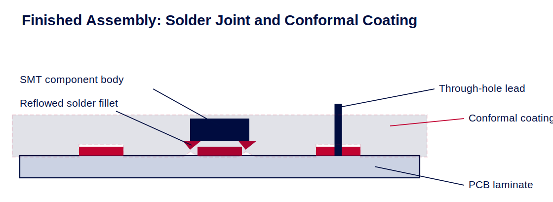
Finished solder joint cross section showing an SMT fillet, a through-hole lead, and conformal coating
From there, the board is integrated into its enclosure if applicable, labeled with serial numbers or traceability markings, and packaged — usually in anti-static, moisture-controlled materials — for shipment. At this point it has gone from a bare board to a finished, tested product.
Turnkey, Consigned, or Somewhere In Between
Assembly houses generally offer three sourcing arrangements, and the right one depends on how much control a customer wants over the supply chain:- Full turnkey means the assembler sources every component and manages the entire process from procurement through shipment. It's the fastest path and shifts sourcing risk onto the assembler, at the cost of less customer control over exactly which parts get used.
- Consigned assembly flips that: the customer supplies every component, and the assembler handles placement, soldering, testing, and inspection. This suits customers with existing supplier relationships or parts on hand, but shifts compatibility risk back to the customer if a supplied part doesn't meet spec.
- Partial turnkey (or COIN — customer-owned inventory) splits the difference: the customer supplies specific hard-to-source or preferred parts, while the assembler sources and manages everything else.
PCB Assembly Process Summary
PCB assembly transforms a bare printed circuit board into a fully functional electronic assembly through a series of carefully controlled manufacturing processes. From design review and solder paste printing to automated component placement, soldering, inspection, testing, and final packaging, every step is designed to ensure the finished assembly meets the required electrical, mechanical, and quality standards. By understanding the complete PCB assembly process, engineers can improve manufacturability, reduce production issues, accelerate product development, and deliver reliable electronic products that perform as intended in the field.
How Printed Circuit Boards Are Assembled: The Complete PCB Assembly Process
A fabricated PCB is just a carrier — copper traces, drilled holes, and a solder mask, but no way to do anything on its own. PCB assembly (often shortened to PCBA) is the process that turns that bare board into a functioning electronic product: mounting components, soldering them in place, and verifying every connection actually works. Fabrication builds the roads; assembly puts the cars on them.
The two stages are handled by different equipment and, often, different facilities. Fabrication produces the copper layers, drills the holes, and applies solder mask and silkscreen. Assembly picks up from there — placing components, either manually or with automated pick-and-place machines, and soldering them using reflow or wave soldering. Since the boards frequently move fab-to-assembly across facilities (or even companies), a clean handoff of files and data matters as much as the physical process itself.
Whether you're developing a new electronic product, selecting a manufacturing partner, or learning how circuit boards are built, understanding the PCB assembly process helps engineers make better design decisions and improve manufacturability. Knowing how components are placed, soldered, inspected, and tested can reduce production issues, improve product reliability, simplify troubleshooting, and accelerate the transition from prototype to full-scale production.
PCB Assembly Process at a Glance
Printed circuit board assembly (PCBA) transforms a bare PCB into a fully functional electronic assembly by mounting, soldering, inspecting, and testing electronic components. While the exact process varies depending on the product, component mix, production volume, and reliability requirements, most PCB assemblies follow the same core manufacturing workflow.
- Design Review and Manufacturing Data Preparation. Manufacturing files, the bill of materials (BOM), pick-and-place data, and assembly drawings are reviewed to verify design-for-manufacturability (DFM) and design-for-assembly (DFA) requirements before production begins.
- Solder Paste Printing. A precision stencil deposits controlled amounts of solder paste onto the PCB pads where surface-mount components will be installed.
- SMT Component Placement. Automated pick-and-place machines accurately position surface-mount components onto the solder paste deposits using vision-guided alignment.
- Reflow Soldering. The populated PCB passes through a controlled reflow oven where the solder paste melts and forms permanent electrical and mechanical connections.
- Inspection. Solder Paste Inspection (SPI), Automated Optical Inspection (AOI), and X-ray inspection verify solder quality, component placement, and hidden solder joints before assembly continues.
- Through-Hole Assembly. Through-hole components are installed and soldered using wave soldering, selective soldering, or hand soldering, depending on the design requirements.
- Cleaning. Flux residues and other contaminants are removed when required to improve long-term reliability and prepare the assembly for testing or conformal coating.
- Electrical Testing and Final Inspection. In-Circuit Testing (ICT), Flying Probe Testing (FPT), functional testing, and final visual inspection verify that the completed assembly meets electrical, mechanical, and quality requirements.
- Conformal Coating, Packaging, and Shipment. When specified, protective coatings, EMI shielding, labeling, and traceability markings are applied before the finished assemblies are packaged using ESD-safe materials and prepared for shipment.
Before Assembly Starts: Files, Standards, and Design Review
Assembly runs on data, not intuition. A complete assembly package includes Gerber or ODB++ files (board geometry), a bill of materials (BOM) listing every part with its manufacturer number and package type, pick-and-place (CPL/centroid) files giving the X/Y coordinates, rotation, and side for every component, NC drill files, and a solder paste stencil file. Miss one, and the risk is real: reversed polarity, missing parts, or components mounted in the wrong spot.Before any board is loaded onto a line, DFA/DFM engineers review this package — checking component footprints against actual part dimensions, spacing between parts, drill-file alignment, thermal relief on pads, and edge clearance. Catching a problem here costs a design revision; catching it after assembly starts costs scrapped boards. This review also flags any incoming quality control (IQC) issues with sourced components before they reach the line.
The workmanship itself is measured against established standards: IPC-A-610 (acceptability criteria for solder joints, component placement, and overall workmanship), IPC-J-STD-001 (materials and methods for soldered assemblies), IPC-7711/7721 (rework and repair procedures), and ISO 9001 (general quality management). A shop citing these isn't just checking a compliance box — they define exactly what a “good enough” solder joint or placement looks like.
Below is the assembly process for a standard board carrying both surface-mount and through-hole components, start to finish.
Ten-step PCB assembly process flow from design review through packaging and shipment
Surface Mount Technology (SMT) Assembly
Most modern boards are populated primarily with surface-mount components — parts soldered directly onto pads on the board surface rather than through drilled holes. SMT allows smaller, denser designs, supports components on both sides of the board, and is built for automation, which is why it dominates high-volume assembly.Solder paste printing
The process starts by depositing solder paste — a mixture of powdered metal solder and flux — onto the exposed copper pads. A thin stainless-steel stencil, laser-cut with an opening over every pad, sits directly on the board; a squeegee blade drags paste across the stencil, filling each aperture, and lifting the stencil leaves clean, precisely sized deposits behind.Three-step solder paste stencil printing process: align, print, lift
Solder paste inspection (SPI)
Before any components go on, automated SPI equipment checks the printed paste. 2D systems measure the height and width of each deposit; 3D systems add volume, giving a more complete picture. Either way, this step catches missing paste, insufficient volume, or bridging between pads before it becomes a soldering defect.Component placement
A pick-and-place machine takes over next, lifting components from tape, tube, or tray feeders, checking orientation and polarity with a built-in vision system, and setting each part onto its paste deposit. High-throughput lines place tens of thousands of components an hour, which is what makes dense, mixed-component boards economical to build at all.Reflow soldering
The populated board then travels through a reflow oven on a conveyor, following a controlled temperature profile that ramps up, melts the solder paste, and cools it back down. Peak temperatures depend on the paste: roughly 180–220°C for leaded solder, 210–250°C for lead-free. As the paste cools, it forms a solid metallurgical bond between each component lead and its pad.Component placement and reflow soldering: pick-and-place followed by the reflow oven
Inspecting the SMT Board
With components soldered, the board goes through inspection before anything else touches it.Automated Optical Inspection (AOI) uses high-resolution cameras to compare the assembled board against a reference image, flagging missing components, wrong orientation, lifted leads, solder bridges, or insufficient solder. It's fast enough to check every board on a production line without slowing throughput.
X-ray inspection picks up where AOI's cameras can't see — specifically, solder joints hidden underneath a component body. Ball grid arrays (BGAs) and other leadless packages solder from underneath, so their joints are invisible to a camera but show up clearly on an X-ray, revealing voids, insufficient solder, or misalignment that would otherwise go undetected until the board failed in the field.
AOI, X-ray, and ICT/flying probe inspection methods used in PCB assembly
Through-Hole Assembly
Some components — connectors, large capacitors, transformers — need more mechanical strength than a surface-mount pad can provide. These use through-hole technology (THT): leads pass through drilled holes and are soldered to pads on the opposite side, which handles physical stress and repeated connector insertion far better than a purely SMT joint.Three soldering methods cover THT assembly, and a single board may use more than one:
- Wave soldering passes the populated board over a standing wave of molten solder, soldering every through-hole lead on the underside in a single pass. It's the standard choice for boards with a meaningful number of THT parts.
- Selective soldering directs a nozzle to solder specific holes one at a time, using robotic positioning instead of a full wave. It's used when only a few THT components are present on an otherwise SMT-heavy board, or when nearby SMT parts can't tolerate the wave.
- Hand soldering covers components too sensitive, too large, or too oddly placed for automated methods, and is also the default for prototypes and very low volumes.
Wave soldering, selective soldering, and hand soldering compared side by side
Mixed-technology boards — carrying both SMT and THT parts — always run SMT first, since it depends on precise placement and reflow heat; through-hole components go on afterward and are soldered using whichever of the three methods fits.
Cleaning and Non-Washable Components
Once soldering is complete, the board is washed typically with deionized water jets, run at controlled temperature and pressure to remove flux residue and other contaminants left behind by soldering. Residue left on the board isn't just cosmetic: it can degrade electrical insulation and long-term reliability.Some components can't tolerate this wash cycle. These non-washable parts are set aside earlier in the process and soldered afterward, typically by hand, using no-clean flux that doesn't require a post-solder wash.
This step is skipped if using a no-clean process.
Final Testing and Inspection
A board that looks right under a camera still has to prove it works electrically.In-Circuit Testing (ICT) uses a bed-of-nails fixture, a grid of spring-loaded pins that contact predefined test points across the board simultaneously, to check for shorts, opens, and correct component values. It's fast and thorough but requires building a custom fixture, which makes sense for higher-volume runs and less sense for a one-off prototype.
Flying Probe Testing (FPT) achieves much the same result without a fixture: one or more probes move freely across the board's surface, contacting test points in sequence based on the design's netlist. It's slower per board than ICT but far more flexible, since there's no hardware to build or retool between design revisions, making it the natural choice for prototypes and lower-volume runs.
Functional testing goes a step further, powering the board and verifying it performs its intended function end-to-end, sometimes alongside burn-in testing for products with high reliability requirements.
Conformal Coating, Shielding, and Final Packaging
For boards headed into harsh environments, a few protective steps come after testing:Conformal coating applies a thin protective layer — acrylic, silicone, polyurethane, epoxy, or vapor-deposited parylene, depending on the required chemical and moisture resistance — over the finished assembly to guard against moisture, dust, and chemical exposure. Each material trades off differently between protection level, cost, and how easily the coating can be reworked later.
Shield cover assembly adds a metallic cover — aluminum, copper, or stainless steel — over sensitive areas of the board to block electromagnetic interference (EMI), both keeping outside EMI from disrupting the board and containing the board's own emissions so they don't interfere with neighboring devices. The cover is typically soldered, clipped, or adhered in place.
Finished solder joint cross section showing an SMT fillet, a through-hole lead, and conformal coating
From there, the board is integrated into its enclosure if applicable, labeled with serial numbers or traceability markings, and packaged — usually in anti-static, moisture-controlled materials — for shipment. At this point it has gone from a bare board to a finished, tested product.
Turnkey, Consigned, or Somewhere In Between
Assembly houses generally offer three sourcing arrangements, and the right one depends on how much control a customer wants over the supply chain:- Full turnkey means the assembler sources every component and manages the entire process from procurement through shipment. It's the fastest path and shifts sourcing risk onto the assembler, at the cost of less customer control over exactly which parts get used.
- Consigned assembly flips that: the customer supplies every component, and the assembler handles placement, soldering, testing, and inspection. This suits customers with existing supplier relationships or parts on hand, but shifts compatibility risk back to the customer if a supplied part doesn't meet spec.
- Partial turnkey (or COIN — customer-owned inventory) splits the difference: the customer supplies specific hard-to-source or preferred parts, while the assembler sources and manages everything else.
PCB Assembly Process Summary
PCB assembly transforms a bare printed circuit board into a fully functional electronic assembly through a series of carefully controlled manufacturing processes. From design review and solder paste printing to automated component placement, soldering, inspection, testing, and final packaging, every step is designed to ensure the finished assembly meets the required electrical, mechanical, and quality standards. By understanding the complete PCB assembly process, engineers can improve manufacturability, reduce production issues, accelerate product development, and deliver reliable electronic products that perform as intended in the field.
Browse
All Categories
Recent Posts
View Recent Posts