


PCB Designs That Work

Good PCB designs must carry signals and power reliably while also fitting the enclosure, managing heat, supporting assembly, and remaining practical to manufacture.
A board can work perfectly in a CAD tool and still be difficult or expensive to fabricate. Problems such as inadequate spacing, poor via selection, unrealistic tolerances, incorrect footprints, or an incomplete fabrication package can lead to engineering questions, manufacturing delays, lower yields, and redesigns.
This guide covers the fundamentals of PCB designs, from stackup and component placement through routing, design for manufacturability (DFM), documentation, and production release.
What Is PCB Design?
PCB design is the process of converting an electronic schematic into the physical layout used to manufacture a printed circuit board.
The designer determines where components are placed, how signals and power are routed, how layers are arranged, and how the board interfaces mechanically with the finished product.
Most PCB designs fall into three basic categories:
- Single-sided PCBs have conductive circuitry primarily on one side and are commonly used for relatively simple designs.
- Double-sided PCBs have copper circuitry on both sides, with plated through-holes commonly used to connect the two sides.
- Multilayer PCBs contain multiple copper layers separated by dielectric materials. They provide more routing space and allow designers to dedicate layers to signals, power, and ground.
As circuit density and electrical performance requirements increase, PCB construction can also incorporate blind and buried vias, microvias, controlled impedance, high-density interconnect (HDI), and specialized materials.
What Makes a Good PCB Design?
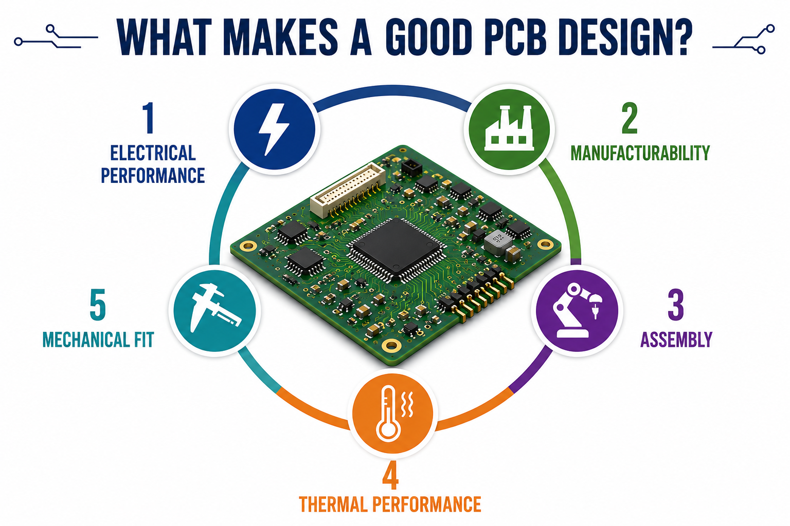
A successful PCB design must satisfy several requirements at the same time.
Electrical performance: Traces, planes, vias, and component placement must support the required current, voltage, signal speed, and impedance.
Manufacturability: Trace widths, spacing, holes, annular rings, solder mask features, and other geometries must fall within the PCB fabricator's capabilities.
Assembly: Component footprints, spacing, polarity markings, fiducials, and test access must support reliable placement, soldering, inspection, and rework.
Thermal performance: Heat must be moved away from power components and other heat-generating devices without exceeding component or material limits.
Mechanical fit: Board dimensions, connectors, mounting holes, component heights, and keep-out areas must match the enclosure and final product.
A strong design addresses these requirements together rather than solving them independently.
Good PCB Design Elements
Start PCB Designs With the Stackup
For multilayer PCB designs, establish the stackup before completing the layout. See PCB Stackup Resources.
The stackup defines the number and arrangement of copper and dielectric layers. It affects board thickness, routing, impedance, electromagnetic performance, manufacturability, and cost.Determine:
- Layer count
- Signal and plane assignments
- Finished board thickness
- Copper thickness
- Dielectric materials and thicknesses
- Controlled impedance requirements
- Via structure
- Minimum trace and space requirements
This is one reason early communication with your PCB manufacturer matters. Changing the stackup after routing is complete can force significant layout changes.
PCB Trace Width, Spacing, and Current
Trace geometry should be based on electrical requirements and manufacturing capability. For signal traces, consider impedance, voltage, frequency, loss, and crosstalk. Power conductors must also be sized for the required current and acceptable temperature rise.
IPC-2152 provides guidance on the relationship between conductor dimensions, current, and temperature rise in printed-board designs. Importantly, current capacity depends on more than trace width alone. Copper thickness, surrounding copper, board construction, and thermal environment also affect conductor temperature.
Clearance also matters. Higher voltages can require greater conductor spacing, while dense low-voltage designs may be limited primarily by fabrication capability. Do not automatically select the smallest trace and space your manufacturer can produce. Designs closer to standard manufacturing capabilities are generally easier and more economical to produce consistently.
Component Placement Comes Before Routing
Good routing begins with good placement.
Start with components that have fixed mechanical locations, such as connectors, switches, mounting holes, and displays. Then position major ICs and their closely associated circuitry.
Keep decoupling capacitors close to the power pins they support and minimize loop inductance. Place switching power components to keep high-current switching loops compact.
High-speed interfaces require additional planning. Memory, clocks, processors, FPGAs, and high-speed connectors should be positioned so critical routes can remain short and maintain suitable reference paths.
For RF designs, antenna keep-out areas and RF routing requirements should be established before general placement fills the available space.
Placement should also consider assembly. Components need enough clearance for manufacturing, inspection, and potential rework.
Routing for Signal and Power Integrity
Once placement is stable, routing turns the schematic connections into physical conductors.
High-speed signals require particular attention to their return paths. Signals should remain referenced to an appropriate continuous plane wherever practical. Unnecessary layer transitions and discontinuities can increase return-path impedance and contribute to noise and electromagnetic interference.
For differential pairs, maintain the geometry required to achieve the target impedance and manage pair skew according to the interface requirements. Avoid unnecessary stubs and via transitions.
Power distribution deserves equal attention. Use suitable power and ground structures, place decoupling capacitors close to the loads they support, and keep high-current paths short and appropriately sized.
Analog and digital circuitry should be placed to control noise and current paths. Avoid automatically splitting ground planes; a poorly positioned plane split can interrupt a signal's return path and create signal-integrity or EMI problems. See "Approaches to PCB Design for Signal Integrity" for more details.
Via Selection in PCB Designs
Vias connect circuitry between layers, but not every design requires advanced via structures.
Through vias extend through the entire PCB and are generally the simplest and most economical option.
Blind vias connect an outer layer to one or more internal layers without passing completely through the PCB.
Buried vias connect internal layers and are not visible from the outside of the finished board.
Microvias are commonly laser drilled and are used extensively in HDI designs.
Blind, buried, and microvia structures can create additional routing space, but they also increase fabrication complexity and cost. Use them when density or electrical requirements justify them.
For rigid PCB designs, IPC-2221 and IPC-2222 provide important design guidance. IPC identifies IPC-2221C as the current generic printed-board design standard and IPC-2222B as the current sectional standard for rigid organic printed boards.
Design PCB Layouts for Manufacturing
Design for Manufacturability should begin during layout, not after the design is finished.
Before committing to detailed routing, confirm your PCB manufacturer's capabilities for:
- Minimum trace and space
- Minimum finished hole and drill sizes
- Annular rings
- Copper-to-edge spacing
- Solder mask registration
- Board thickness and thickness tolerance
- Controlled impedance
- Blind, buried, and microvia structures
- Surface finishes
- Materials and copper weights
These capabilities are not identical at every PCB manufacturer.
A DFM review before production can identify features that are technically possible but difficult to manufacture consistently. Small changes made before release can prevent engineering holds and improve production yield.
Relevant IPC Standards for PCB Designs
Several IPC standards are particularly useful when developing professional PCB designs.
IPC-2221C – Generic Standard on Printed Board Design
Provides generic design requirements applicable across printed-board technologies.
IPC-2222B – Sectional Design Standard for Rigid Organic Printed Boards
Provides requirements specifically for rigid PCB design, including electrical, mechanical, thermal, and physical design considerations.
IPC-2152 – Standard for Determining Current Carrying Capacity in Printed Board Design
Provides guidance for evaluating conductor size, current, and temperature rise. IPC currently lists this document as no longer maintained, but it remains an established technical reference.
IPC-7351 – Surface Mount Design and Land Pattern Standard
Provides guidance for surface-mount land-pattern geometry and considers factors including solder joints, inspection, testing, and rework.
IPC-6012F – Qualification and Performance Specification for Rigid Printed Boards
This is a fabrication performance specification rather than a PCB design standard, but designers should understand it when specifying the required performance class and acceptance requirements for rigid boards.
The correct standards and performance requirements should be identified in the procurement documentation rather than assumed by the manufacturer.
Thermal Management in PCB Design
Thermal design should begin during component placement. Copper areas can help spread heat from power devices. Thermal vias can conduct heat between layers or toward larger copper areas, depending on the board construction. Heatsinks, thermal interface materials, airflow, chassis connections, and other cooling methods may also be required.
Do not assume that adding more thermal vias automatically solves a thermal problem. Via geometry, copper thickness, layer structure, component thermal characteristics, and the complete heat path all matter. For higher-power designs, thermal simulation and physical testing can help verify performance under realistic operating conditions.
Prototype and Validate Before Production
Prototype builds allow engineers to verify that the PCB works as intended before committing to production quantities.
Testing should address the risks specific to the product and may include:
- Power-up and functional testing
- Signal-integrity measurements
- Thermal testing
- Mechanical fit
- EMI/EMC evaluation
- Programming and firmware verification
- Boundary scan
- Environmental or reliability testing
Use prototype results to improve the design. A board that functions electrically may still benefit from changes that improve manufacturability, testability, thermal performance, or production yield. Before final release, run another DFM and Design for Assembly (DFA) review.
What Files Does a PCB Manufacturer Need?
A complete manufacturing package reduces questions and prevents assumptions during CAM review.
For PCB fabrication, provide:
|
File or Document |
Typical Information |
|---|---|
|
PCB image data |
Gerber or another manufacturer-supported fabrication data format |
|
Drill data |
Plated and non-plated hole information |
|
Fabrication drawing |
Dimensions, tolerances, notes and special requirements |
|
Stackup |
Layer order, materials, and copper requirements |
|
Impedance requirements |
Controlled-impedance values and applicable tolerances |
|
Surface finish |
ENIG, ENEPIG, HASL, OSP, immersion silver, etc. |
|
Netlist |
Used for electrical verification when required |
If assembly is also being quoted, provide the BOM, centroid/pick-and-place data, assembly drawings, paste-layer data, and applicable test or programming requirements separately.
IPC also identifies IPC-2614 for board fabrication documentation and IPC-2615 for printed-board dimensions and tolerances.
PCB Design Checklist
Before releasing PCB designs for manufacturing, verify:
- Stackup has been reviewed with the PCB manufacturer.
- Materials and copper requirements are clearly defined.
- Trace/space and hole sizes meet manufacturing capabilities.
- Controlled-impedance requirements are identified.
- Power and high-current conductors are appropriately sized.
- Critical signals have continuous return paths.
- Component footprints have been verified.
- Board dimensions and mechanical interfaces match the enclosure.
- Fabrication notes and tolerances are complete.
- Fabrication and drill data use the same coordinate origin.
- Applicable IPC class and customer requirements are identified.
- A final DFM review has been completed.
From PCB Design to Manufacturing
The best PCB designs balance electrical performance, mechanical requirements, thermal management, assembly, and manufacturability from the beginning.
One of the most effective ways to reduce manufacturing problems is also one of the simplest: involve your PCB manufacturer early. Review the stackup, materials, impedance requirements, trace and space, via structures, and other critical features before the layout is locked.
A design that works electrically is only part of the goal. A production-ready PCB design should also be repeatable and practical to manufacture at the required quality level.