


PCB Fabrication Drawing
Posted
8/17/2026
.png?resizemode=force&maxsidesize=500)
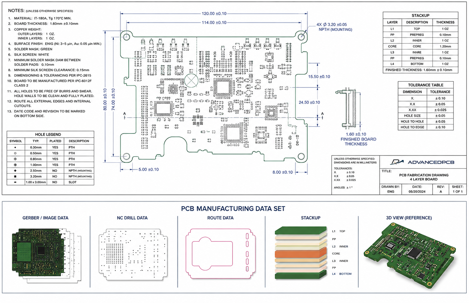
A fabrication drawing, sometimes called a fab drawing or fabrication blueprint, tells a PCB manufacturer how the finished bare printed circuit board should be built. It works alongside the electronic manufacturing data to define the board's physical dimensions, materials, construction, tolerances, surface finish, special features, and other requirements that may not be fully communicated by the PCB image and drill data alone.
Think of the fabrication drawing as part of the manufacturing contract between the designer and PCB fabricator. The electronic data defines the circuitry and holes. The fabrication drawing provides additional information needed to interpret that data and manufacture the finished board to the intended requirements.
A clear fabrication drawing reduces assumptions during CAM review, helps prevent engineering holds, and gives both the customer and PCB manufacturer a common reference for determining whether the finished board meets specification.
IPC-2614, Sectional Requirements for Board Fabrication Documentation, establishes requirements for documenting PCB fabrication and identifies physical attributes and performance requirements for the unpopulated board. The standard applies to rigid, flexible, multilayer, HDI, and other PCB constructions.
A fabrication drawing typically works with manufacturing files such as:
A good fabrication blueprint helps answer important manufacturing questions before production begins:
What material should be used?
The drawing can identify laminate requirements, material specifications, or approved alternatives.
How thick should the finished PCB be?
Finished board thickness and applicable tolerance can be specified.
What surface finish is required?
ENIG, ENEPIG, immersion silver, OSP, HASL, or another specified finish can be called out.
Which dimensions are critical?
Board outline dimensions, cutouts, slots, hole locations, and tolerances can be clearly identified.
What performance requirements apply?
IPC performance class, controlled impedance, electrical test, inspection, and other customer-specific requirements can be identified where applicable.
Without clear documentation, the fabricator may need to stop the order and request clarification.
IPC-2615 addresses practices for dimensioning and tolerancing printed boards, while IPC-2614 addresses the broader fabrication documentation package. IPC's revision table notes that fabrication drawing requirements previously associated with IPC-D-325 were superseded by IPC-2614.
IPC-A-600 provides visual interpretations of externally and internally observable printed board conditions and is used with applicable performance specifications such as IPC-6012.
Do not simply put "build to IPC standards" on a fabrication blueprint. Identify the applicable specification, revision when required by your procurement system, performance class, and any customer-specific requirements.
IPC documentation describes the master or fabrication drawing as defining the unpopulated printed board and the features that become part of that board, while an assembly drawing identifies components associated with the assembly.
For a bare-board order, assembly information should not be used as a substitute for a complete PCB fabrication package.
That becomes increasingly important as PCB complexity increases. Multilayer stackups, controlled impedance, HDI structures, specialized materials, tight mechanical tolerances, and high-reliability requirements leave less room for assumptions.
Good fabrication documentation will not make a difficult PCB simple to manufacture. It does something equally important: it makes the requirements clear before
Think of the fabrication drawing as part of the manufacturing contract between the designer and PCB fabricator. The electronic data defines the circuitry and holes. The fabrication drawing provides additional information needed to interpret that data and manufacture the finished board to the intended requirements.
A clear fabrication drawing reduces assumptions during CAM review, helps prevent engineering holds, and gives both the customer and PCB manufacturer a common reference for determining whether the finished board meets specification.
What Is a PCB Fabrication Drawing?
A PCB fabrication drawing is a controlled document that describes the requirements for manufacturing an unpopulated printed circuit board.IPC-2614, Sectional Requirements for Board Fabrication Documentation, establishes requirements for documenting PCB fabrication and identifies physical attributes and performance requirements for the unpopulated board. The standard applies to rigid, flexible, multilayer, HDI, and other PCB constructions.
A fabrication drawing typically works with manufacturing files such as:
- Gerber or other PCB image data
- NC drill and route data
- Netlist data
- Stackup information
- Controlled impedance requirements
- Additional customer specifications
Why Is a Fabrication Drawing Important?
PCB manufacturing requires more information than copper artwork alone can communicate. For example, image data can show where copper should appear, but it may not clearly define the required finished board thickness, material system, surface finish, dimensional tolerances, impedance requirements, hole tolerances, plating requirements, or acceptance criteria. That information can be communicated through the fabrication drawing.A good fabrication blueprint helps answer important manufacturing questions before production begins:
What material should be used?
The drawing can identify laminate requirements, material specifications, or approved alternatives.
How thick should the finished PCB be?
Finished board thickness and applicable tolerance can be specified.
What surface finish is required?
ENIG, ENEPIG, immersion silver, OSP, HASL, or another specified finish can be called out.
Which dimensions are critical?
Board outline dimensions, cutouts, slots, hole locations, and tolerances can be clearly identified.
What performance requirements apply?
IPC performance class, controlled impedance, electrical test, inspection, and other customer-specific requirements can be identified where applicable.
Without clear documentation, the fabricator may need to stop the order and request clarification.
What Should Be Included in a PCB Fabrication Drawing?
The exact information depends on the PCB, but a professional fabrication drawing commonly includes several categories of information.
1. Board Dimensions and Mechanical Features
Define the finished board outline and critical mechanical dimensions. These may include:- Overall length and width
- Board thickness
- Cutouts
- Slots
- Notches
- Edge features
- Critical hole locations
- Countersinks or counterbores when required
- Dimensional tolerances
IPC-2615 addresses practices for dimensioning and tolerancing printed boards, while IPC-2614 addresses the broader fabrication documentation package. IPC's revision table notes that fabrication drawing requirements previously associated with IPC-D-325 were superseded by IPC-2614.
2. PCB Stackup
For multilayer boards, the stackup defines how the layers are arranged. Depending on the design and procurement requirements, fabrication documentation may identify:- Number of layers
- Layer order
- Copper requirements
- Dielectric materials
- Finished board thickness
- Controlled-impedance structures
- Special construction requirements
3. Material Requirements
The fabrication drawing should clearly communicate required PCB materials when material selection is important to performance. Rather than relying only on a generic callout such as "FR-4," specifications may need to address characteristics such as:- Material specification
- Tg requirements
- Dk/Df requirements
- Thermal performance
- UL requirements
- Halogen-free requirements
- CAF resistance
- Customer-approved material systems
4. Hole and Via Requirements
The NC drill data identifies hole locations and sizes, but the fabrication drawing can provide additional requirements needed to interpret those holes correctly. This can include:- Finished hole sizes and tolerances
- Plated versus non-plated holes
- Slots
- Blind and buried vias
- Microvias
- Via filling
- Via plugging
- Via capping
- Countersinks and counterbores
5. Copper and Plating Requirements
The fabrication blueprint should define applicable copper requirements. Depending on the design, these can include:- Starting or finished copper requirements
- Copper plating requirements
- Edge plating
- Plated slots
- Via fill
- Copper-filled vias
- Special plating requirements
6. Surface Finish
The required final surface finish should be clearly identified. Common choices include:- ENIG
- ENEPIG
- Lead-free HASL
- HASL
- Immersion silver
- Immersion tin
- OSP
7. Controlled Impedance Requirements
If the PCB contains controlled-impedance circuits, include the required impedance information in the manufacturing package. This may identify:- Single-ended impedance targets
- Differential impedance targets
- Applicable tolerance
- Relevant layer or trace structures
- Coupon or test requirements
8. Solder Mask and Legend Requirements
Fabrication documentation may specify:- Solder mask type
- Solder mask color
- Mask requirements
- Legend or marking color
- Special marking requirements
- Areas where markings are prohibited
9. PCB Acceptance and IPC Requirements
A fabrication drawing should identify applicable acceptance requirements. For rigid printed boards, IPC-6012F establishes qualification and performance requirements. It covers single-sided, double-sided and multilayer rigid boards, including constructions with blind vias, buried vias, and microvias. IPC-6012F recognizes three general performance classes based on customer or end-use requirements.IPC-A-600 provides visual interpretations of externally and internally observable printed board conditions and is used with applicable performance specifications such as IPC-6012.
Do not simply put "build to IPC standards" on a fabrication blueprint. Identify the applicable specification, revision when required by your procurement system, performance class, and any customer-specific requirements.
Fabrication Drawing vs. Assembly Drawing
These documents serve different purposes and should not be confused.
| Fabrication Drawing | Assembly Drawing |
|---|---|
| Defines the bare PCB | Defines the populated assembly |
| Board dimensions and tolerances | Component locations |
| Materials and stackup | Reference designators |
| Holes, slots and cutouts | Component orientation |
| Surface finish | Polarity information |
| Fabrication requirements | Assembly instructions |
| PCB acceptance requirements | Assembly-specific requirements |
For a bare-board order, assembly information should not be used as a substitute for a complete PCB fabrication package.
Fabrication Drawing vs. Gerber Files
A fabrication drawing and Gerber data also serve different purposes. Gerber data primarily represents PCB image information. The fabrication drawing communicates manufacturing requirements that may not be apparent from the artwork alone. For example, Gerber data may show a board outline and copper features, but it does not necessarily tell the manufacturer:- The required finished board thickness
- The material requirements
- Which dimensional tolerances are critical
- The required surface finish
- The performance class
- Controlled-impedance targets
- Special via processing requirements
- Customer-specific acceptance criteria
Common Fabrication Drawing Mistakes
Many PCB manufacturing delays are caused not by difficult technology, but by unclear or conflicting documentation. Watch for these problems:- Conflicting dimensions: The drawing specifies a dimension that does not match the electronic data.
- Missing tolerances: A critical mechanical feature is dimensioned without defining the allowable variation.
- Ambiguous material callouts: The drawing uses a broad material description even though the design requires specific electrical or thermal properties.
- Unclear copper requirements: It is not clear whether the specified copper thickness refers to starting copper or finished copper.
- Missing impedance information: The files indicate controlled-impedance traces but do not provide clear targets or tolerances.
- Outdated revisions: The fabrication drawing, drill data, and image files come from different PCB revisions.
- Unnecessary notes: Old fabrication notes are copied from another design even though they do not apply to the current board.
How to Create a Better Fabrication Drawing
A useful fabrication drawing is clear, specific, and easy for CAM engineers to interpret. Before releasing your design:- Verify the drawing revision matches the manufacturing data.
- Confirm dimensions against the actual PCB outline.
- Identify critical tolerances rather than applying unnecessarily tight tolerances everywhere.
- Review the stackup with the PCB manufacturer.
- Clearly define materials and surface finish.
- Identify applicable IPC performance requirements.
- Include controlled-impedance requirements where applicable.
- Verify drill and route requirements.
- Remove obsolete or conflicting notes.
- Run a DFM review before releasing the board for production.
Why Fabrication Drawings Matter
A PCB fabricator should not have to guess what the designer intended. A well-prepared fabrication drawing connects the electronic design to the physical PCB that comes off the manufacturing floor. It communicates dimensions, materials, construction, tolerances, finishes, special processing, and acceptance requirements in a controlled format.That becomes increasingly important as PCB complexity increases. Multilayer stackups, controlled impedance, HDI structures, specialized materials, tight mechanical tolerances, and high-reliability requirements leave less room for assumptions.
Good fabrication documentation will not make a difficult PCB simple to manufacture. It does something equally important: it makes the requirements clear before
FAQs for Fabrication Drawings
Is a fabrication drawing the same as a fabrication blueprint?
What is a fabrication drawing for a PCB?
What is the difference between a fabrication drawing and an assembly drawing?
What should be included in a PCB fabrication drawing?
Do I need a fabrication drawing if I have Gerber files?
Browse
All Categories
Recent Posts
View Recent Posts