

PCB Material Selection: How to Choose the Right Materials in a High-Demand, Supply-Constrained Market

PCB material selection has become more critical than ever as demand from AI infrastructure, data centers, and high-speed computing continues to strain global supply chains. Lead times for certain laminates, prepregs, and copper foils have increased, and availability can vary by region and supplier. This makes material selection not just a design decision, but a supply chain strategy.
This guide from AdvancedPCB explains how to choose the right PCB materials, what properties matter most, how to balance performance with availability, and which IPC standards support reliable results. If you are evaluating PCB materials for high-speed, power-dense, or reliability-critical designs, this article covers material types, key properties, stackup strategies, and best practices for navigating both technical and supply challenges.
Understanding PCB Materials
PCB materials provide the structure and insulation that allow electrical signals and power to flow through copper traces. A typical PCB stackup includes dielectric laminates, prepregs, copper foil, bonding materials, and a surface finish.
These materials directly affect:
- Signal integrity and impedance control
- Thermal performance and heat dissipation
- Mechanical strength and durability
- Manufacturability and yield
- Long-term reliability
Choosing the wrong material can lead to signal loss, overheating, warpage, or reliability failures. That’s why PCB material selection is one of the most important decisions in board design.
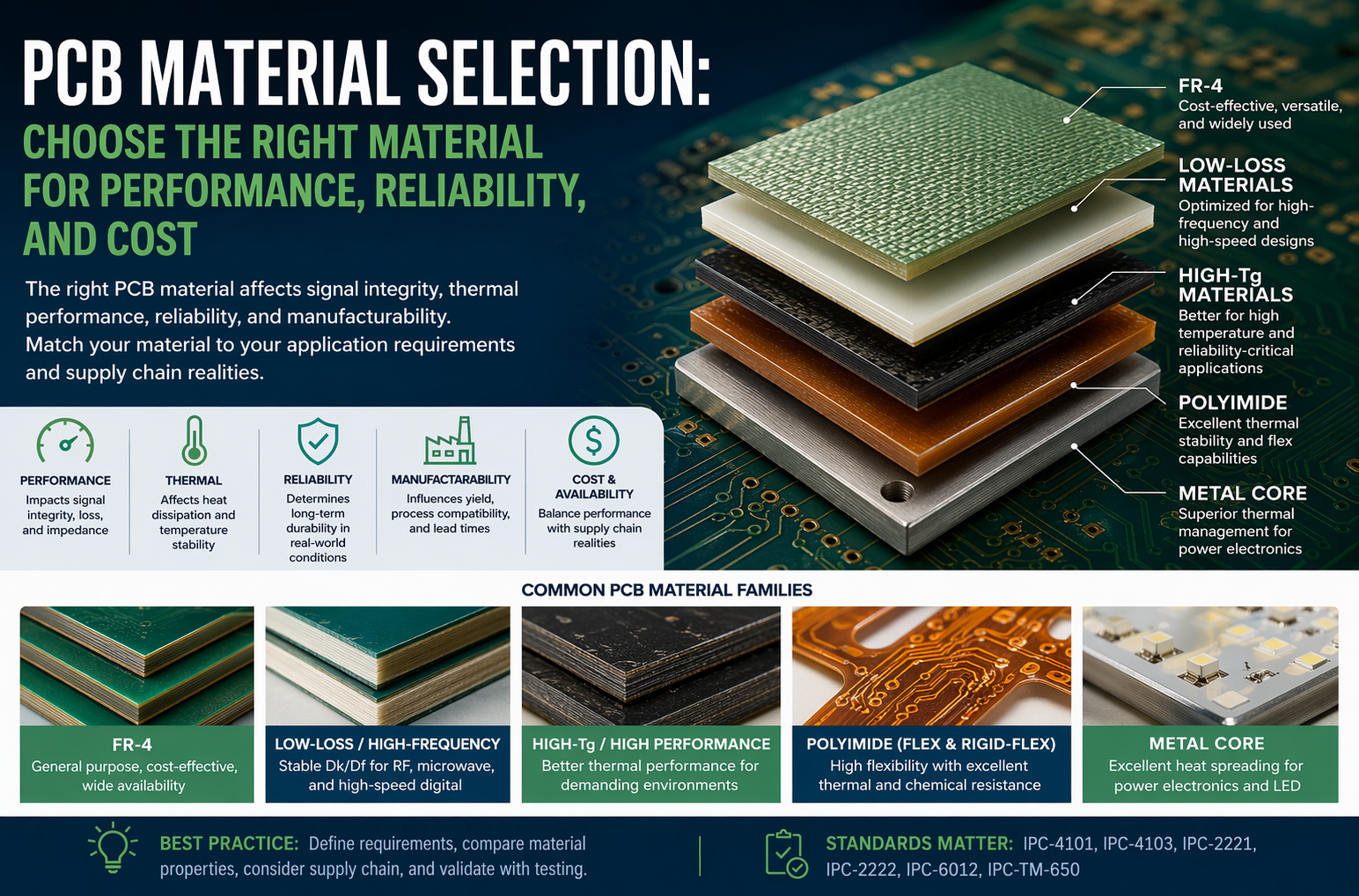
What Are the Most Common PCB Material Types?
FR-4: The industry workhorse for a broad range of applications due to its balance of cost, manufacturability, and mechanical strength. Enhanced variants include lead-free compatible, high-Tg, and lower-loss epoxies. For multi-gigabit systems up to about 10–14 Gbps over moderate distances, improved FR-4 grades may suffice. Beyond that, consider mid-/low-loss FR-4 derivatives or hybrid stackups integrating RF-capable cores for critical paths. FR-4 remains the baseline PCB material for many cost-sensitive products.
High-frequency materials: PTFE-based laminates, hydrocarbon-ceramic composites, and advanced low-loss epoxies provide stable Dk and low Df for RF, microwave, and mmWave designs. These materials typically feature tight dielectric tolerance and offer smoother copper foil options to reduce conductor loss. They are prevalent in 5G radios, phased arrays, satellite links, radar systems, and precision timing networks. To manage cost, many designs use high-frequency cores only where necessary and rely on FR-4 elsewhere, a common approach in PCB materials selection for mixed-signal platforms.
High-thermal-performance epoxies and polyimide: For power conversion, automotive underhood, and high-reliability sectors, high-Tg epoxies and polyimides withstand repeated thermal excursions and maintain mechanical integrity. Polyimide excels in extreme temperatures and demanding thermal cycles but often comes at higher cost and can require specialized processing. When choosing material for PCB assemblies that face frequent thermal shocks, these resin systems are often favored.
Flexible and rigid-flex materials: Flex circuits use polyimide films that support tight bending and dynamic motion, ideal for compact devices, wearables, medical electronics, and aerospace harness replacements. Rigid-flex combines rigid sections for component mounting with flexible interconnects to reduce connectors, improve reliability, and enable three-dimensional packaging. Key variables include minimum bend radius, dynamic flex life, adhesiveless versus adhesive constructions, and coverlay selection. These circuit board materials open design freedom where space and reliability are at a premium.
If you are comparing types of PCB materials for a new platform, map your performance needs to the families above and shortlist specific grades that meet both electrical and process constraints.
Key Properties of PCB Materials
Dielectric Constant (Dk)
Dk determines how fast signals travel through the material and affects impedance. Stable Dk across frequency and temperature is critical for high-speed designs.
Loss Tangent (Df)
Df measures how much signal energy is lost as heat. Lower Df means less signal loss, which is important for high-speed and RF applications.
Thermal Properties
Key values include:
- Tg (glass transition temperature)
- Td (decomposition temperature)
- CTE (coefficient of thermal expansion)
These affect how the board behaves during soldering and temperature cycling.
Mechanical and Processing Properties
Factors like moisture absorption, resin flow, copper adhesion, and CAF resistance all impact manufacturability and long-term reliability.
How Do You Choose the Right PCB Material?
Material selection should follow a structured approach.
Start with:
- Signal speed and frequency requirements
- Power density and thermal conditions
- Environmental exposure (humidity, vibration, temperature)
- Mechanical constraints
Then evaluate:
- Dk and Df performance at your operating frequency
- Thermal properties for assembly and operation
- Reliability factors like CAF resistance and moisture absorption
- Supply availability and lead times
In many cases, a hybrid stackup is the best solution, using high-performance materials only where needed.
Comparing Common Material Options
| Material Family | Typical Dk (1-10 GHz) | Typical Df | Thermal Notes | Use Cases |
|---|---|---|---|---|
| Standard FR-4 | ~4.1–4.6 | ~0.016–0.020 | Moderate Tg; suitable for single reflow; lower thermal conductivity | General-purpose digital, consumer, industrial control |
| Low-/mid-loss FR-4 derivatives | ~3.6–4.2 | ~0.008–0.014 | High-Tg available; better z-axis stability; improved loss | High-speed digital up to mid-teens Gbps, moderate reach |
| Hydrocarbon-ceramic | ~2.9–3.5 | ~0.003–0.008 | Good processability; improved thermal conductivity vs. FR-4 | RF/microwave, 5G radios, phased arrays |
| PTFE-based | ~2.1–2.6 | ~0.0009–0.003 | Excellent stability; specialized processing; low CTE options | Microwave/mmWave, satellite, precision timing |
| Polyimide | ~3.2–3.8 | ~0.010–0.015 | Very high Tg/Td; robust thermal cycling | High temperature, aerospace, power electronics |
| Flex polyimide (adhesiveless) | ~3.1–3.5 | ~0.008–0.012 | Thin cores; high bend endurance; tailored copper treatments | Wearables, medical, compact electronics, rigid-flex |
Values vary by supplier and copper foil type; always consult frequency-specific data and confirm tolerances for your operating band and thermal profile. When comparing types of PCB materials, use measured data from relevant frequencies and copper profiles to make apples-to-apples decisions.
.png "ChatGPT-Image-Apr-16,-2026,-01_06_39-PM-(1).png")
Which IPC Standards Apply to PCB Material Selection?
Several IPC standards support material selection and reliability:
- IPC-4101
- IPC-4103
- IPC-2221
- IPC-2222
- IPC-6012
- IPC-TM-650
These standards help ensure materials meet performance, reliability, and manufacturing requirements.
Stackup Strategies and Hybrid Builds
Few designs need premium materials across every layer. A hybrid approach concentrates low-loss or RF-qualified cores in the critical signal paths while using cost-effective FR-4 for the remaining layers. Key considerations include:
- Resin compatibility and press temperature alignment to ensure proper bonding and minimal voiding.
- CTE matching to mitigate stress at interfaces between dissimilar materials, preserving via reliability.
- Copper foil selection with appropriate roughness where conductor loss is limiting and standard foils elsewhere for cost and adhesion.
- Impedance modeling across the hybrid transitions, especially for buried stripline in mixed dielectric sections.
When material availability is tight, hybrid builds also create alternatives: if a specific low-loss core is allocated, a functionally equivalent grade can sometimes be substituted in the limited layers without disrupting the rest of the stack. These strategies should be part of any PCB material selection guide focused on resilience and cost control.
Signal Integrity, Copper Foil, and Weave Effects
At multi-gigabit rates, conductor loss and dielectric loss both matter. Copper foil roughness increases skin-effect losses, and the choice between very low profile (VLP), low profile (LP), or reverse-treated foils affects both loss and adhesion. For the most demanding channels, smoother foils can yield measurable improvements in insertion loss and eye opening. Selecting circuit board materials with compatible foil treatments is a practical lever in PCB materials selection for high-speed designs.
Glass weave may introduce skew when differential pairs traverse resin and glass regions unevenly. Techniques to mitigate weave-induced skew include using spread or flat weaves, choosing glass styles with tighter resin fill, rotating the routing angle slightly relative to the weave, or pairing materials known for weave uniformity. Always validate through-time skew and eye performance with test coupons that reflect the actual routing geometry. These considerations often guide the material for PCB stackups in networking and data center products.
Supply Chain Planning Amid Material Shortages
Market conditions have tightened availability for specific laminates, prepregs, and copper foils. To minimize risk:
- Create a dual-source AVL with validated equivalents for key layers, including matched Dk/Df and similar press cycles.
- Lock in forecasts with suppliers early and confirm lead times for both core materials and foils; some grades may require extended bookings.
- Define acceptable tolerance bands for Dk and foil roughness on drawings, enabling substitutions within a controlled performance envelope.
- Where possible, design stackups that can accept two or three closely matched laminates without layout changes, and maintain test data for each.
- Coordinate with your fabricator on inventory holdings and regional supply constraints to avoid last-minute redesigns.
An actionable PCB materials selection plan accounts for volatility, maintains pre-qualified alternates, and embeds flexibility into documentation to keep programs on schedule.
Summary
PCB material selection is no longer just a technical decision. It is a balance between performance, reliability, manufacturability, and supply chain risk.
The best approach is to:
- Define requirements clearly
- Use data-driven material selection
- Validate with testing and prototypes
- Build flexibility into your design
- Place a purchase order early so the PCB manufacturer can secure materials in parrallel with finalizing your design
By combining strong engineering practices with supply chain awareness, you can select PCB materials that meet both performance goals and production realities.
Related Posts

FR-4: The Essential Guide to PCB Substrate Material

Circuit Boards: A Guide to Choosing Materials
