


High-Density Interconnect PCBs (HDI)
EHDI PCBs are the enabling technology behind the most compact, capable electronics being built today — from sub-millimeter-pitch BGA packages to implantable medical devices and mission-critical avionics. We manufacture high-density interconnect boards with the precision processes, engineering depth, and quality controls your program demands, from first prototype through volume production.
Our U.S.-based manufacturing capabilities support high-power PCB applications where thermal reliability, current density, and long-term system performance
.jpg)
What Is an HDI PCB?
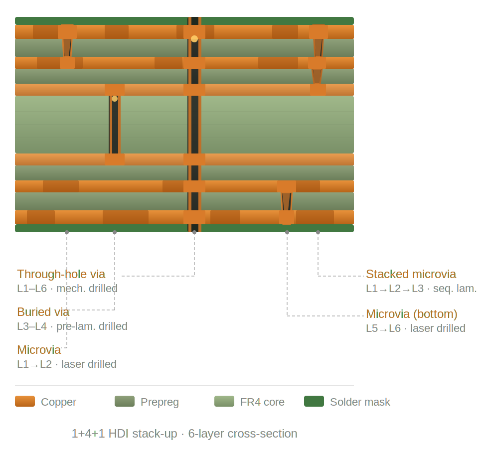
A high-density interconnect PCB achieves greater wiring density than conventional boards through a combination of fine lines and spaces, thin dielectrics, laser-drilled microvias, and sequential build-up (SBU) lamination. Where standard multilayer boards rely on mechanical through-holes, HDI uses blind vias, buried vias, and stacked or staggered microvia structures to pack significantly more interconnections into the same or smaller board outline.
Typical HDI characteristics include:
- Laser-drilled microvias typically under 150 microns (6 mil) in diameter
- Trace and space down to 3/3 mil or finer
- Stacked or staggered via structures built across multiple lamination cycles
- Thin dielectrics enabling tighter impedance control and increased interplane capacitance for improved performance
When HDI Makes Sense
HDI is the right choice when your design requires:
- Fine-pitch BGA fan-out
Packages at 0.5 mm pitch and below require microvia escape routing that through-hole vias simply can't provide. - Complex designs in tight mechanical envelopes
When your board outline is fixed and layer count needs to stay manageable, HDI routing efficiency is often the only path forward. - High-speed signal integrity
Shorter interconnects, reduced via stubs, and finer geometries minimize parasitic inductance and capacitance on high-speed serial, RF, and mixed-signal interfaces. - Consolidation of multiple boards
HDI often allows two or more conventional PCBs to be integrated into a single board, reducing assembly complexity, connector count, and overall system cost.
Although HDI introduces additional fabrication complexity, improved routing efficiency can often reduce total layer count, connector count, and overall system cost.
Core HDI Technologies
- Microvias. Laser-drilled to connect adjacent layers, microvias are the foundation of HDI routing. Stacked microvias maximize routing density but require tight process control and validated copper fill to ensure long-term thermal cycling reliability. Staggered configurations offset vias between layers to reduce reliability risk in certain stack-up configurations.
- Blind and Buried Vias. Blind vias connect an outer layer to one or more inner layers without traversing the full board thickness. Buried vias connect only internal layers, freeing outer layer real estate for dense component placement and fine-pitch fan-out.
- Via-in-Pad. Required under fine-pitch BGAs to shorten escape routing, via-in-pad demands resin-filled and copper-capped vias to produce flat, solderable pads.
- Sequential Lamination. Common stack-up configurations are built through multiple lamination cycles, each adding laser-drilled microvia layers to the core. This is the process that makes HDI's routing density possible. Each sequential lamination cycle introduces additional thermal exposure, making copper balance, resin flow control, and registration accuracy critical to long-term reliability.
HDI Design Considerations
HDI rewards thoughtful upfront planning. Key factors that determine performance and manufacturability:
- Stack-up and material selection. Laminate choice affects signal performance, thermal stability, dimensional control, and cost. High-speed or thermally demanding designs often call for high-Tg FR-4 or mid/low-loss laminates with compatible prepregs. Thinner dielectrics support impedance targets and increase plane capacitance for better power delivery. PCB laminate guide >
- Via strategy and copper balance. Effective stacking and fill specifications, realistic microvia dimensions, and balanced copper distribution across layers reduce warpage during lamination and improve interconnect reliability through thermal cycling.
- Signal integrity. Maintain consistent impedance on critical traces, place reference planes adjacent to high-speed layers, and keep return paths short. As via stubs shrink with HDI structures, parasitic inductance drops and signal performance improves measurably.
- Thermal management. HDI condenses heat sources. Plan thermal vias, copper pours, and heat spreaders accordingly, and ensure copper balance to prevent warpage.
- DFM alignment. Maintain appropriate clearances around microvias, specify via fill requirements explicitly, use consistent design grids, and plan test point access. Provide complete fabrication data — Gerber or ODB++, drill files including separate laser drill files, impedance tables, and full stack-up notes — for accurate quoting and clean release to production.
- IPC standards.
- IPC-2226 provides HDI-specific design guidance covering microvias, sequential lamination, via structures, and high-density routing strategies.
- IPC-6016 defines qualification and performance requirements specifically for high-density interconnect structures and microvia reliability.
- IPC-6012 Class 3 requirements are commonly applied in aerospace, defense, and medical HDI applications requiring enhanced reliability.
- HDI laminates are commonly selected according to IPC-4101 governing dielectric performance, thermal properties, CAF resistance, and dimensional stability.
- Reliability validation may include IPC-TM-650 test methods for thermal stress, interconnect integrity, and conductive anodic filament (CAF) resistance.
Industries and Applications
HDI technology is found at the heart of the most demanding electronics across every major sector:
Aerospace & Defense
Avionics, ruggedized electronics, ITAR-regulated programs requiring rigorous qualification and traceability
Learn moreAI & Data Centers
AI accelerators, high-speed servers, and networking platforms require advanced PCB fabrication
Learn moreMedTech
Implantable devices, surgical instruments, miniaturized diagnostics where board size is directly constrained by the human body
Learn moreIndustrial & Robotics
Compact connected devices that demand high functionality in constrained form factors
Learn moreTelecom & Datacom
High-speed line cards, optical modules, and infrastructure equipment where signal integrity is non-negotiable
Learn more
HDI Manufacturing Capabilities
We build high-density interconnect boards with the process discipline and inspection rigor that complex designs require. Some of AdvancedPCB's HDI tolerances and capabilities include:
| HDI Capabilities | ||
|---|---|---|
| Total Pad Size | Typical | Advanced |
| Capture Pad | Drill + 0.008 | Drill + 0.006 |
| Landing Pad | Drill + 0.008 | Drill + 0.006 |
| BC Mechanical Drill (Type III) | 0.008 | 0.006 |
| Material Thickness | 0.004-0.010 | 0.0025 |
| Stacked Via | 0.0035 | 0.0025 |
| Type I Capabilities Single & Double Deep | Yes | Yes |
| Type II Capabilities Buried Vias with Microvias | Yes | Yes |
| Type III Capabilities | Yes | Yes |
| Copper Filled Microvias | Yes | Yes |
| Smallest Copper Filled Microvia | 0.004 | 0.0025 |
| Copper Filled Microvia Hole Size | 0.75:1 | 1:1 |
| Smallest Laser Microvia Hole Size | 0.004 | 0.0025 |
| Laser Via Aspect Ratio (Depth: Diameter) | 0.75:1 | 1:1 |
Why Choose AdvancedPCB for HDI PCBs?
- Proven experience with microvia processes including reliable copper fill and cap.
- Engineering team engaged throughout your project.
- Proactive DFM feedback to resolve issues prior to fabrication.
- Rigorous in-process quality validation at every build stage.
- Transparent pricing driven by real cost factors such as layer count, material class, and more.
- On-time delivery your program schedule can depend on.
Partner With Us Early
HDI designs have less margin for late-stage changes than standard boards, which makes involving us early one of the best decisions you can make for your program. Our engineers work with your team before production begins: reviewing stack-up construction, co-developing design rules, flagging DFM issues, and recommending materials that balance performance, manufacturability, and budget.
Whether you're in early development, scaling an existing design, or qualifying for a regulated industry, we're equipped to support you at every phase.