


AdvancedPCB Strengthens Aurora Manufacturing with New Strip-Etch-Strip Line
Posted
7/22/2026
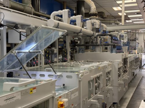
AdvancedPCB has installed a new Strip-Etch-Strip (SES) wet-process line at its Aurora, Colorado manufacturing facility. The investment is part of the company's 2026 Technology Acceleration Initiative to strengthen manufacturing capabilities and support the production of increasingly advanced printed circuit boards (PCBs).
The installation was completed during a scheduled production shutdown over the Independence Day holiday weekend, minimizing disruption to customer production schedules.
The SES process is a key step in PCB inner-layer fabrication, where copper circuitry is formed before the layers are bonded together. Consistent control during this process is essential for maintaining accurate line widths, spacing, and registration before lamination. As PCB designs continue to incorporate finer features, higher layer counts, and tighter tolerances, precise inner-layer processing plays an increasingly important role in overall board quality and manufacturability.


Supplied by Equip Tech and manufactured by Universal Circuit Board Equipment Co. (UCE), the SES line incorporates automated chemical management, conveyorized material handling, and integrated process controls throughout the strip, etch, and strip cycle. The new system is designed to support a broad range of PCB technologies, including HDI, multilayer, and other high-density circuit board designs.
"PCB designs continue to become more complex, and it's our responsibility to invest ahead of our customers' needs," said Greg Halvorson, Chief Executive Officer at AdvancedPCB. "The SES line is one of several manufacturing investments we're making throughout 2026 to ensure our facilities are equipped to support the next generation of electronics while delivering the quality, responsiveness, and manufacturing expertise our customers depend on."
AdvancedPCB's Aurora, Colorado facility specializes in quick-turn PCB fabrication and prototype assembly, supporting customers from early product development through low-to-mid-volume production. The facility's continued growth is driving ongoing investments in new manufacturing technologies and infrastructure. As one of the largest equipment investments made at the Aurora facility in recent years, the new SES line reflects AdvancedPCB's long-term commitment to expanding its capabilities in Aurora.
The SES line is one of several strategic investments AdvancedPCB is making across its network of US-based manufacturing facilities. By continuing to invest in advanced equipment and process technologies, the company is expanding its ability to support customers in designing and manufacturing the next generation of aerospace & defense, medical, AI and data center infrastructure, industrial, and consumer electronics.
Click here for more details on our capabilities.
The installation was completed during a scheduled production shutdown over the Independence Day holiday weekend, minimizing disruption to customer production schedules.
The SES process is a key step in PCB inner-layer fabrication, where copper circuitry is formed before the layers are bonded together. Consistent control during this process is essential for maintaining accurate line widths, spacing, and registration before lamination. As PCB designs continue to incorporate finer features, higher layer counts, and tighter tolerances, precise inner-layer processing plays an increasingly important role in overall board quality and manufacturability.
Supplied by Equip Tech and manufactured by Universal Circuit Board Equipment Co. (UCE), the SES line incorporates automated chemical management, conveyorized material handling, and integrated process controls throughout the strip, etch, and strip cycle. The new system is designed to support a broad range of PCB technologies, including HDI, multilayer, and other high-density circuit board designs.
"PCB designs continue to become more complex, and it's our responsibility to invest ahead of our customers' needs," said Greg Halvorson, Chief Executive Officer at AdvancedPCB. "The SES line is one of several manufacturing investments we're making throughout 2026 to ensure our facilities are equipped to support the next generation of electronics while delivering the quality, responsiveness, and manufacturing expertise our customers depend on."
AdvancedPCB's Aurora, Colorado facility specializes in quick-turn PCB fabrication and prototype assembly, supporting customers from early product development through low-to-mid-volume production. The facility's continued growth is driving ongoing investments in new manufacturing technologies and infrastructure. As one of the largest equipment investments made at the Aurora facility in recent years, the new SES line reflects AdvancedPCB's long-term commitment to expanding its capabilities in Aurora.
The SES line is one of several strategic investments AdvancedPCB is making across its network of US-based manufacturing facilities. By continuing to invest in advanced equipment and process technologies, the company is expanding its ability to support customers in designing and manufacturing the next generation of aerospace & defense, medical, AI and data center infrastructure, industrial, and consumer electronics.
Click here for more details on our capabilities.
Browse
All Categories
Recent Posts
View Recent Posts