

PCB X-Ray Inspection: How Manufacturers Verify Hidden Solder Joints and Internal PCB Quality

PCB X-ray inspection is one of the most powerful tools available for verifying solder joint quality, identifying hidden defects, and ensuring long-term reliability in electronic assemblies. Unlike optical inspection methods, X-ray systems can see beneath components and inside multilayer circuit boards, revealing defects that would otherwise remain hidden until product testing or field failure.
From BGAs and QFNs to plated through-holes and internal vias, X-ray inspection plays a critical role in modern PCB manufacturing, assembly, failure analysis, and quality assurance.
This guide explains how PCB X-ray inspection works, what defects it can identify, and why it has become an essential part of high-reliability electronics manufacturing.
Related resources:
- PCB Assembly Services
- HDI PCB Manufacturing
- Design for Manufacturability (DFM)
- TruView Novus X-Ray System
Why PCB X-Ray Inspection Matters
Traditional visual inspection and Automated Optical Inspection (AOI) are effective for evaluating visible solder joints and component placement. However, many critical connections are hidden beneath components or embedded within the PCB structure. X-ray inspection allows manufacturers to examine these concealed features without cutting, damaging, or reworking the assembly.
Common applications include:
- BGA solder joint inspection
- QFN and LGA package analysis
- Through-hole solder verification
- Via and barrel crack evaluation
- Solder void measurement
- Internal layer inspection
- Failure analysis and root-cause investigations
For aerospace, defense, medical, automotive, and industrial electronics, X-ray inspection provides documentation and traceability that support both quality requirements and customer confidence.
How PCB X-Ray Inspection Works
PCB X-ray systems pass controlled radiation through an assembly and capture the resulting image using a high-resolution detector. Because different materials absorb X-rays differently, solder joints, copper features, vias, and component structures become visible as varying shades within the image. Several inspection methods are commonly used:
- 2D X-Ray Inspection: A standard 2D image provides a top-down view of the assembly and is commonly used for routine production inspection and defect detection.
- 2.5D Inspection: Also known as laminography or oblique-angle inspection, 2.5D systems generate multiple angled views that help isolate overlapping features and improve analysis of complex assemblies.
- 3D Computed Tomography (CT); CT scanning reconstructs hundreds of images into a three-dimensional model that allows engineers to examine internal structures layer by layer. This capability is especially valuable for failure analysis, void quantification, and advanced package inspection.
Defects X-Ray Inspection Can Detect
One of the greatest advantages of X-ray inspection is its ability to reveal defects that cannot be seen through optical methods. Common defects include:
- BGA voiding
- Head-in-pillow defects
- Open solder joints
- Insufficient solder volume
- Bridging
- Barrel cracks
- Lifted pads
- Delamination
- Internal fractures
- Excessive voiding beneath thermal pads
These issues can significantly impact reliability, particularly in assemblies subjected to thermal cycling, vibration, or harsh operating environments.
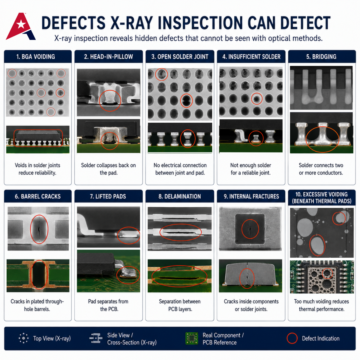.png "X-Ray-inspection-defects-(2).png")
X-Ray Inspection for BGA and QFN Assemblies
BGA and QFN packages are among the most common reasons manufacturers utilize X-ray inspection. Because solder joints are hidden beneath the package body, visual inspection cannot adequately verify connection quality. X-ray imaging allows inspectors to evaluate solder ball shape, alignment, voiding levels, and overall joint integrity without removing the component. For QFN packages, X-ray inspection is often used to assess voiding beneath the exposed thermal pad, which can affect both thermal performance and long-term reliability.
Automated X-Ray Inspection
Modern Automated X-Ray Inspection systems use software algorithms to analyze solder joints and compare results against predefined acceptance criteria.
These systems can automatically evaluate:
- Solder volume
- Void percentage
- Ball diameter
- Joint alignment
- Component placement
- Pass/fail criteria
By integrating inspection results with manufacturing execution systems (MES), manufacturers can improve traceability and support continuous process improvement.
IPC Standards and X-Ray Inspection
Several IPC standards influence how X-ray inspection is used during PCB assembly and quality verification.
- IPC IPC-A-610 provides acceptability criteria for electronic assemblies and is commonly referenced when evaluating solder joint quality.
- IPC IPC-7095 offers guidance for BGA design and assembly processes, including inspection considerations.
- IPC IPC-7093 addresses bottom-terminated components such as QFN and DFN packages where X-ray inspection is frequently required.
These standards help establish consistent acceptance criteria across manufacturing environments.
AdvancedPCB's X-Ray Inspection Capabilities
As electronic assemblies become more complex, inspection technology must evolve to keep pace. AdvancedPCB recently expanded its inspection capabilities with the installation of the TruView Novus X-Ray System. The system provides high-resolution imaging for hidden solder joints, BGAs, QFNs, vias, and other critical assembly features.
By incorporating advanced X-ray inspection into our manufacturing process, we can identify defects earlier, improve traceability, and provide customers with greater confidence in assembly quality and reliability.
Improving Reliability Through Better Inspection
PCB X-ray inspection has become a critical quality tool for modern electronics manufacturing. Its ability to reveal hidden solder joints, internal defects, and structural issues allows manufacturers to identify problems before products reach the field. Whether inspecting BGAs, evaluating QFN thermal pads, verifying via integrity, or supporting failure analysis, X-ray inspection provides insights that traditional inspection methods cannot. As package densities continue to increase and assemblies become more complex, advanced X-ray inspection will remain one of the most important technologies for ensuring PCB quality, reliability, and long-term performance.