

Blind Buries Vias PCB: Key Manufacturing Insights

Blind and buried vias are a key topic in modern printed circuit board (PCB) manufacturing, especially as designs become smaller and more complex. Below, we’ll explain what blind and buried vias are, how they’re created by a PCB manufacturer, and how they can help you achieve the electrical performance and layout density your design requires. We’ll also cover PCB via advantages, fabrication considerations, and why partnering with an experienced PCB shop is essential when your design calls for these advanced via structures.
As component density increases, it’s often impossible to route every required connection on a single PCB layer. Vias solve this problem. A via is a plated, conductive hole—essentially a small copper-lined barrel—that allows signals and power to move from one copper layer to another. While there are several via types, blind and buried vias are among the most important for high-density designs, and they can provide significant benefits when implemented correctly by a qualified PCB manufacturer.
What is the Difference Between Blind and Buried Vias?
A blind via connects an external layer of the PCB to one or more inner layers but does not pass completely through the board. It “starts” on an outer surface and “ends” on an internal layer. A buried via, on the other hand, is located entirely within the PCB stackup and connects only inner layers; it is not visible from either outer surface. For comparison, a standard through-hole via extends from the top layer to the bottom layer and ties together every layer it intersects. Although the concepts are straightforward, the choice between blind, buried, and through-hole vias has important implications for routing density, signal integrity, and manufacturability.
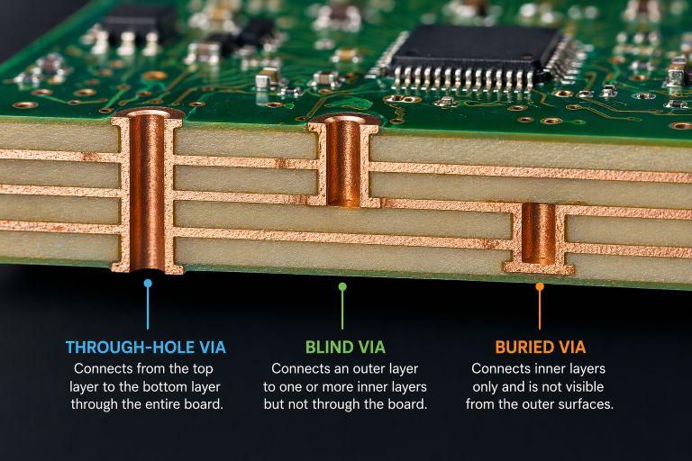.jpg "Vias-Diagram-(1).jpg")
Many Benefits of Blind and Buried Vias
Because many modern PCBs are compact and densely populated, blind and buried vias are often used to reclaim valuable surface area. Buried vias free up routing space on the outer layers by moving some of the interconnections into the internal layers, without interfering with surface components or traces. Blind vias provide additional routing flexibility by allowing connections from fine-pitch devices—such as BGA packages—directly into the inner layers without occupying space on the opposite side of the board. Since blind vias only traverse a portion of the stackup, they also reduce unused via stubs, which can improve signal integrity at higher frequencies.
Blind and buried vias are especially common in high-density interconnect (HDI) PCBs. HDI technology enables tighter trace/space rules, more interconnections per unit area, and improved power distribution. By using blind and buried vias, designers can shrink overall board size and weight while still meeting complex routing requirements—an important advantage in compact products. As a result, HDI boards with blind and buried vias are widely used in smartphones, tablets, laptops, medical electronics, wearables, and other small or lightweight devices.
However, these advanced via types do add complexity and cost to PCB fabrication. Multiple lamination cycles, precision drilling, and additional inspection steps are usually required. For this reason, blind and buried vias should be used strategically—only where they provide clear benefits in terms of performance, miniaturization, or routing feasibility. A good PCB manufacturer can help you balance design goals against cost and manufacturability.
How Are the Blind and Buried Vias Built?
Blind and buried vias can be created either before or during the multilayer lamination process, depending on the stackup and via strategy. In all cases, accurate drilling and plating are critical. A PCB manufacturer must tightly control drill depth to ensure that each via terminates on the intended layer without over- or under-drilling. If the via is too shallow, it may not properly connect to the target copper pad; if it is too deep, it can introduce signal integrity issues, reliability concerns, or unintended connections to other layers.
For blind vias, the PCB manufacturer typically uses a dedicated drill file that defines the start and stop layers for each via type. The aspect ratio—the relationship between the via depth and finished hole diameter—must stay within process limits. Keeping the depth-to-diameter ratio at or below 1:1 for laser-drilled microvias, for example, helps ensure reliable plating and robust connections between the outer layer and the designated inner layer.
Buried vias are formed between inner layers that are laminated together before the full stackup is built. Each buried via set is usually defined in a separate drill file because it connects specific internal layers only. Here again, the via aspect ratio is critical; manufacturers often limit the hole depth-to-diameter ratio to around 10–12:1 or less, depending on equipment and process capability. Exceeding these limits can make plating difficult and increase the risk of defects or shorts to adjacent features.
Working with a capable PCB manufacturer is the best way to confirm that your blind and buried via structures are practical to build. An experienced fabrication team will review your stackup, drill charts, and design files to verify that via sizes, depths, and aspect ratios are within their process window. This upfront review helps prevent costly redesigns, delays, or yield issues later in production.
Skilled manufacturers use controlled-depth drilling, proper desmear and cleaning processes, and optimized plating chemistry to ensure that blind and buried vias are fully formed and free of voids. They also take steps to avoid trapped air or contamination in the via barrels, which can compromise reliability over time.
Choosing a Printed Circuit Board Manufacturer
Because blind and buried vias demand tight process control, your choice of PCB manufacturer is critical. You’ll want a fabricator that has proven experience with HDI technology, controlled-depth drilling, and sequential lamination, and that can clearly explain their capabilities and design rules for advanced vias.
A dependable PCB manufacturer will operate a modern production facility, use up-to-date drilling and imaging equipment, and follow robust process controls to maintain consistency from lot to lot. Look for a partner that offers a thorough engineering design review before fabrication begins. This review should include checks for via aspect ratios, stackup integrity, drill registration, and overall manufacturability so that your boards perform as intended once assembled.
Turnaround time is another important factor. A qualified manufacturer should be able to produce PCBs with blind and buried vias on a predictable schedule, even for complex HDI builds, and provide clear lead-time estimates for prototypes and production runs.
Cost transparency also matters. Choose a PCB supplier that can provide fast, detailed quotes that reflect the added complexity of blind and buried vias, including extra lamination cycles, drilling steps, and inspection. This allows you to make informed tradeoffs between design complexity and budget.
If your design requires blind and buried vias, partnering with an experienced PCB manufacturer can make the process straightforward and reliable. A capable supplier will help you optimize your layout, confirm manufacturability, and deliver high-quality boards that meet your electrical, mechanical, and schedule requirements.

AdvancedPCB
Related Posts

The PCB Fabrication Process

FR-4: The Essential Guide to PCB Substrate Material
