


Single-Layer / Single-Sided PCBs
Simple, cost-effective rigid circuit boards with one copper layer, built for prototype and production quantities.
This page covers single-sided PCBs, also known as single-layer PCBs, and explains when this construction is the right choice for a design. Topics include how a single-sided board is built, why the terms single-layer and single-sided are used interchangeably, advantages and limitations, where to find our manufacturing capabilities, common applications, design considerations, and frequently asked questions.
What Is a Single-Sided PCB?
A single-sided PCB has one layer of copper bonded to one side of a rigid substrate. All traces are routed on that copper side. Through-hole components sit on the bare side with their leads soldered to pads on the copper side, while surface mount components mount directly on the copper side.
Single-Layer vs. Single-Sided: Same Board, Two Names
The two terms describe the same construction. "Single-layer" refers to the number of copper layers, and "single-sided" refers to the copper being on one side of the board. Engineers and buyers use both, and both describe a rigid board with one conductive layer and no plated through holes.
Single-Sided PCB Construction
- Substrate: FR-4 glass-reinforced epoxy, or CEM-1 and CEM-3 for cost-sensitive designs [confirm materials offered]
- Copper foil: One conductive layer, etched to form traces and pads
- Solder mask: Protects copper and prevents solder bridging
- Silkscreen: Component designators, polarity marks, and part numbers
- Surface finish: Protects exposed pads and supports solderability
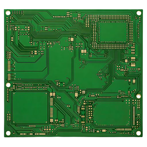
Advantages and Limitations of Single-Sided PCBs
Advantages
- Lowest fabrication cost of any rigid PCB type
- Fewer process steps, which shortens lead times and reduces failure points
- Straightforward visual inspection and troubleshooting
- Well suited to high-volume, cost-driven products
Limitations
- Limited routing density, since traces cannot cross without jumpers
- Larger board area for the same circuit compared with double-sided designs
- No plated holes, so through-hole joints rely on pad adhesion alone
- Not suited to high-speed signals, controlled impedance, or dense packages
Single-Sided PCB Capabilities
Detailed specifications for single-sided PCBs, including board thickness, copper weights, trace and space, drilling, and impedance tolerances, are listed on our Manufacturing Capabilities page. Capabilities can be viewed by facility.
Single-Sided PCB Applications
Single-sided boards remain the practical choice for circuits with low component counts and simple signal paths.
- Power supplies and LED drivers
- LED lighting assemblies
- Sensors and detectors
- Relays and timing circuits
- Calculators, remotes, and simple control panels
- Appliance and consumer electronics
Single-Sided PCB Design Considerations
- Route to minimize jumpers. Every jumper or zero-ohm resistor adds an assembly step, so plan component placement around trace paths early.
- Size pads generously. Without plated holes, through-hole joints depend on pad area and annular ring for mechanical strength.
- Match trace width to current. Use wider traces on power paths to manage temperature rise on a single copper layer.
- Plan panelization for volume. Single-sided designs are often run in arrays, so define rails, fiducials, and breakaway tabs up front.
- Know when to step up. If a layout needs many jumpers, a ground plane, or both-side component placement, a double-sided PCB is usually more cost-effective overall.