PCB Drill Alignment: Why Accurate Hole Positioning Matters
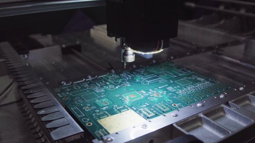
Zccurate PCB drill alignment is essential to producing a printed circuit board that matches the original design. Drilled holes must align correctly with copper pads, internal features, the board outline, slots, and other mechanical features.
Even a small registration error can reduce the remaining annular ring around a drilled hole. More significant misregistration can affect electrical connections, mechanical fit, or the finished board's ability to meet its specified acceptance requirements.
PCB manufacturers use coordinated image, drill, route, and fabrication data to establish where holes and other features belong. Understanding how drill alignment works can help designers prepare cleaner manufacturing files and reduce questions during CAM review.
What Is PCB Drill Alignment?
PCB drill alignment is the registration of drilled hole locations to the other features of a printed circuit board.
Those features can include:
- Copper pads
- Internal-layer features
- Vias
- Component holes
- Mounting holes
- Slots
- Cutouts
- Board edges and other mechanical features
The drill locations are typically provided to the PCB manufacturer through NC drill data. The manufacturer must ensure that this information uses the correct coordinate system and aligns with the rest of the manufacturing data.
The original version of this AdvancedPCB article described using the board edge in relation to a hole location as a reference for aligning the NC drill file. Modern PCB data preparation is broader than that description. CAM systems register the complete manufacturing dataset, and common origins, accurate data, and clearly defined mechanical requirements help prevent alignment errors.
Why Does Drill Alignment Matter?
Consider a plated through-hole surrounded by a copper pad.
Ideally, the drilled hole is positioned near the center of the pad, leaving sufficient copper around the finished hole. That remaining copper is the annular ring.
If the drill shifts relative to the copper feature, the annular ring becomes smaller on one side.
The issue becomes more important as PCB features get smaller. A relatively small registration shift consumes a larger percentage of the available annular ring when pads and holes are tightly sized.
Drill alignment can therefore affect:
- Annular ring
- Hole-to-copper relationships
- Layer-to-layer interconnection
- Mechanical hole locations
- Connector alignment
- Slots and cutouts
- Board-to-enclosure fit
- Finished-board acceptance
Good drill registration is not simply about making a hole appear centered. It is about maintaining the required relationship between the drilled feature and the rest of the PCB.
How NC Drill Files Are Used
An NC drill file provides machine-readable information defining hole locations and drill sizes.
The fabrication package also needs to communicate which holes are plated and non-plated, along with any special requirements for slots, blind or buried vias, microvias, countersinks, counterbores, or other drilled and routed features.
A common coordinate origin across the manufacturing data helps the PCB manufacturer register these datasets correctly.
Problems can occur when:
- Drill and image files use different origins
- Units or coordinate formats are unclear
- Drill data comes from a different design revision
- Plated and non-plated holes are not clearly identified
- Mechanical drawings conflict with NC data
- Slots or special hole requirements are ambiguous
These issues may be discovered during CAM review, but resolving them can delay the order while the manufacturer requests clarification.
Drill Alignment and Annular Ring
Annular ring is one of the most important concepts associated with PCB drill alignment.
The annular ring is the copper surrounding a finished plated hole. Its geometry is influenced by several factors, including the pad diameter, finished hole size, drilling accuracy, plating, and layer-to-layer registration.
Designers should not treat the CAD pad-to-hole relationship as a guarantee of the exact finished annular ring. PCB fabrication involves multiple processes, each with manufacturing tolerances.
This is why the manufacturer's design rules matter.
Using unnecessarily small pads around drilled holes can leave little manufacturing margin. Designing within established fabrication capabilities provides more tolerance for normal process variation.
Drill Alignment in Multilayer PCBs
Drill registration becomes more complex in a multilayer PCB.
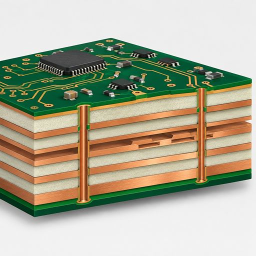
Before drilling, multiple copper and dielectric layers are laminated into a single structure. The drilled hole must then intersect the intended pads on the applicable layers.
Registration is affected by more than drilling-machine positioning. Materials can move dimensionally during processing, and multilayer fabrication requires careful compensation and registration throughout imaging, lamination, and drilling.
PCB manufacturers use process controls and registration systems to account for these effects.
For the designer, the key point is simpler: provide enough design margin for the fabrication process being used.
Very small annular rings, high layer counts, small drilled holes, and dense multilayer structures generally require tighter process control than less aggressive designs.
Plated vs. Non-Plated Holes
Not every drilled hole serves the same purpose.
Plated through-holes (PTHs) have conductive plating on the hole wall. They may provide electrical connections between layers or accommodate through-hole component leads.
Non-plated through-holes (NPTHs) do not receive conductive hole-wall plating and are commonly used for mounting, tooling, or other mechanical purposes.
The distinction needs to be clear in the manufacturing data.
For a plated hole, drill alignment may directly affect the relationship between the hole and its copper pads.
For a mechanical mounting hole, alignment may instead be critical to enclosure hardware, connectors, standoffs, or other physical features.
Both require accurate positioning, but for different reasons.
Drill Alignment and PCB Tolerances
Every PCB manufacturing process has tolerances.
Drilling equipment can achieve high positional accuracy, but the finished relationship between a hole and surrounding features is influenced by the complete manufacturing process. Layer registration, material movement, imaging, lamination, drilling, and plating can all contribute to the final result.
Designers should therefore specify tolerances based on the needs of the product rather than applying extremely tight tolerances to every hole.
A mounting hole used for a loose-fit fastener may not require the same positional control as a precision alignment feature.
Unnecessarily tight tolerances can increase manufacturing complexity and cost without improving product performance.
IPC Requirements and Drill Alignment
IPC standards provide requirements and acceptance criteria relevant to drilled PCB features.
For rigid printed boards, IPC-6012F establishes qualification and performance requirements, including requirements associated with holes, plating, annular ring, and internal structures.
IPC-A-600 provides visual guidance for evaluating printed-board acceptability and includes internally observable conditions associated with plated holes and registration.
For PCB design, IPC-2221 provides generic printed-board design guidance, while IPC-2222 addresses rigid organic printed-board design.
The applicable IPC performance class should be established based on the product's requirements. Designers should also review the PCB manufacturer's capabilities because minimum pad, hole, annular ring, and registration rules can vary by process and technology.
How Designers Can Reduce Drill-Alignment Problems
Many potential drill-alignment issues can be addressed before the PCB reaches manufacturing.
Start with these practices:
- Use the same coordinate origin for PCB image, drill, and route data.
- Verify that all manufacturing files represent the same design revision.
- Clearly distinguish plated and non-plated holes.
- Define critical finished-hole sizes and tolerances.
- Make sure the fabrication drawing agrees with the NC drill data.
- Clearly identify slots and special mechanical features.
- Avoid unnecessarily small annular rings.
- Design within the PCB manufacturer's established capabilities.
- Run a DFM check before releasing the design.
For multilayer, HDI, or tight-tolerance designs, involve the PCB fabricator early. The manufacturer can review pad sizes, drill diameters, annular ring requirements, layer registration, and other features before they become locked into the design.
The Bottom Line
PCB drill alignment is about maintaining the intended relationship between holes and the electrical and mechanical features around them.
Accurate manufacturing data is the starting point. Drill files, PCB image data, route data, dimensions, and fabrication requirements should use consistent coordinates and revisions so the manufacturer has a clear definition of the finished board.
Design margin matters too. Adequate annular rings and realistic hole tolerances give the fabrication process room to accommodate normal manufacturing variation.
For complex or tightly spaced boards, an early DFM review can identify potential drill-registration problems before manufacturing begins. That is much easier than discovering an alignment issue after the boards have already been built.
When you are in the process of designing your printed circuit boards and placing your order, it is important to remember to submit all of the files you will need to help the process go smoothly. At the same time, AdvancedPCB provides you with a comprehensive list of terms used in the industry so you can learn more. A fab drawing, for example, is used in the construction of PCBs and uses the board's edge in relation to at least one hole location as a reference point during the manufacturing stage. This helps align the NC Drill file so that you get the precision you need.
Turn to AdvancedPCB for the Printed Circuit Boards You Need
Whether you have to fulfill a large production quantity or are ordering a small amount of PCBs for a school project, AdvancedPCB has you covered. You can get the standard and custom spec PCBs you need when you need them most from one of the largest manufacturers in the country and the one with the best on-time shipping record in the industry. Contact a representative today to learn how to get your goals achieved quickly and affordably so you never have to sacrifice quality.
.png)
AdvancedPCB
FAQs for Drill Alignment
Related Posts
Why Do PCBs Have an Even Number of Layers?