Why Do PCBs Have an Even Number of Layers?
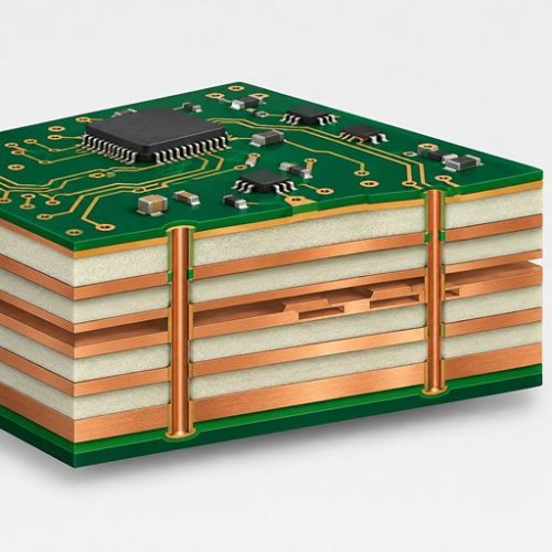
Most multilayer printed circuit boards (PCBs) are manufactured with an even number of copper layers—typically 4, 6, 8, or 10. The primary reason is manufacturing balance. Even-layer constructions make it easier to create symmetrical stackups that reduce board warpage, support consistent dielectric thickness, and improve manufacturing repeatability.
Odd-layer PCBs are possible, but they are less common because they may require additional materials or manufacturing adjustments to achieve a balanced construction.
Why Even-Layer PCB Stackups Are Preferred
A PCB stackup consists of copper layers separated by insulating dielectric materials. Two primary materials form the structure:
- Core: Fully cured laminate, commonly FR-4, typically supplied with copper bonded to both sides. Learn more about laminates >
- Prepreg: Partially cured resin-impregnated fiberglass used to bond copper foils and cores during lamination.
Even-layer designs make it easier to arrange these materials symmetrically around the board's centerline. This helps manufacturers manage three important factors.
1. Reduced Warpage
During lamination, heat and pressure bond the PCB layers together. As the board cools, differences in material expansion and copper distribution can create mechanical stress. A balanced stackup helps reduce bow and twist, improving board flatness during assembly and operation. However, an even number of layers does not guarantee a balanced board. Dielectric thickness, copper distribution, and material selection must also be considered.
2. More Consistent Manufacturing
Standard even-layer constructions allow manufacturers to use established core and prepreg combinations, simplifying material selection and fabrication. Balanced constructions help control dimensional stability and reduce the risk of manufacturing defects associated with excessive board distortion.
3. Greater Stackup Design Flexibility
Even-layer stackups provide practical options for arranging signal, ground, and power layers. For example, a common 4-layer PCB uses:
| Layer | Function |
|---|---|
| L1 | Signal |
| L2 | Ground |
| L3 | Power |
| L4 | Signal |
A 6-layer PCB provides additional options for routing and reference planes.
These arrangements can support controlled impedance, signal integrity, and electromagnetic interference (EMI) management. However, electrical performance depends on the actual layer arrangement and routing—not whether the layer count is even or odd.
Can a Multilayer PCB Have an Odd Number of Layers?
Yes. Odd-layer PCBs, such as 3-layer or 5-layer constructions, are technically possible, but they are generally less common and may be more expensive than comparable standard even-layer designs. An odd-layer construction can make mechanical symmetry more difficult to achieve. Manufacturers may compensate by adjusting dielectric materials, copper distribution, or the lamination structure. In some cases, adding a nonfunctional copper layer to create an even-layer construction may be more economical than manufacturing an unconventional odd-layer stackup.
Engineers should discuss odd-layer requirements with their PCB manufacturer early in the design process to evaluate cost, manufacturability, and available alternatives.
IPC Standards and Multilayer PCB Construction
Several IPC standards are relevant to multilayer PCB design and manufacturing:
- IPC-2221 and IPC-2222: Provide general and rigid-board-specific design requirements, including multilayer construction considerations.
- IPC-4101: Defines specifications for laminate and prepreg materials used in rigid and multilayer PCBs.
- IPC-6012: Establishes qualification and performance requirements for rigid PCBs, including applicable structural integrity and bow-and-twist requirements.
These standards help engineers specify reliable PCB constructions, but they do not universally require an even number of layers.
Choosing the Right Multilayer PCB Stackup
Before finalizing a stackup, engineers should consider the required layer count, signal and power plane assignments, finished board thickness, copper weights, dielectric materials, and controlled-impedance requirements. Working with your PCB manufacturer early helps ensure the selected construction meets electrical and mechanical requirements without introducing unnecessary manufacturing complexity. AdvancedPCB provides PCB stackup resources and engineering support to help customers select appropriate layer constructions, materials, and dielectric thicknesses for their designs.
.png)
AdvancedPCB
FAQS on Why PCBs Have Even Layers
Related Posts

Heavy Copper PCBs for Automotive Electronics: Design Considerations

Built for the Factory Floor