


High Density Interconnect (HDI) PCBs: A Complete Guide
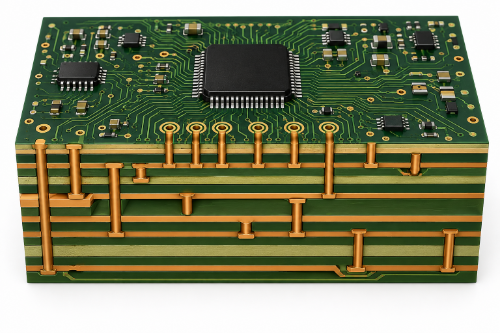
High density interconnect (HDI) is a printed circuit board technology used to fit more electrical connections into a smaller area. HDI PCBs combine fine conductors, small vias, thin dielectric layers, and advanced multilayer construction to support high-density components and complex routing.
The technology is especially useful when a conventional through-hole PCB cannot provide enough routing space for fine-pitch BGAs, high pin-count devices, or compact electronics.
HDI is not simply about making a PCB smaller. A successful high density interconnect design requires the stackup, microvias, materials, routing, and fabrication processes to work together. This guide explains how HDI PCBs work, where they provide an advantage, and what engineers should consider before designing one.
What Is High Density Interconnect?
High density interconnect is a PCB technology that achieves greater interconnection density than conventional printed circuit boards by using features such as microvias, fine lines and spaces, thin dielectric layers, and sequential build-up structures.
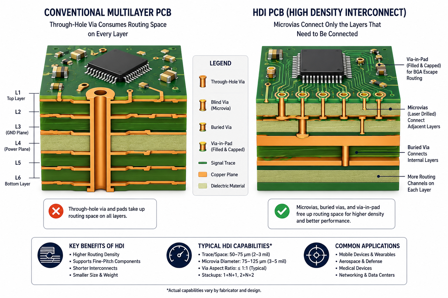
Microvias are one of the defining features of HDI. IPC terminology defines a microvia as a blind or subsequently buried hole less than 0.15 mm (0.006 in.) in diameter that is formed and subsequently metallized. Microvias are commonly created using laser drilling.
Common HDI features include:
- Microvias: Small vias used to connect adjacent or selected layers.
- Blind vias: Vias that connect an outer layer to one or more inner layers without passing through the entire PCB.
- Buried vias: Vias located completely within the multilayer structure.
- Via-in-pad: A via placed directly within a component pad, often to provide routing access beneath fine-pitch BGAs.
- Fine lines and spaces: Smaller conductors and clearances that allow more routing channels in a limited area.
- Sequential lamination: Multiple lamination and drilling cycles used to build HDI layers around a multilayer core.
How Does an HDI PCB Differ From a Conventional PCB?
A conventional multilayer PCB relies heavily on mechanically drilled plated through-holes that extend through the entire board. Those holes consume routing space on every layer they pass through. HDI changes that approach. Microvias, blind vias, and buried vias can connect only the layers that require an electrical transition. This leaves additional routing space available on other layers.
A common HDI stackup might be described as 1+N+1, meaning one HDI build-up layer is added to each side of a conventional multilayer core. A 2+N+2 construction uses two sequential build-up layers on each side. As HDI complexity increases, manufacturing complexity usually increases as well. Additional lamination, imaging, laser drilling, metallization, plating, and registration steps can affect cost, lead time, and yield.
What Are the Benefits of High Density Interconnect?
The primary benefit of high density interconnect is routing density.Smaller PCB Size
Microvias and finer routing allow designers to place components closer together and route signals through areas that would be difficult to access with conventional through-holes. This can reduce PCB size or allow additional functionality within an existing footprint.
Support for Fine-Pitch Components
Current processors, FPGAs, memory devices, and other high-I/O components often use fine-pitch BGA packages. HDI techniques such as via-in-pad can provide escape routing when conventional dog-bone fanouts no longer fit between BGA pads.
Shorter Signal Paths
Microvias can reduce interconnect length and eliminate unnecessary through-hole via stubs. When the stackup and return paths are designed correctly, this can help reduce parasitic effects and support signal integrity in high-speed designs. HDI alone does not guarantee better signal integrity. Impedance geometry, reference planes, materials, return paths, via transitions, and routing still have to be engineered correctly.
Reduced Size and Weight
Smaller vias, thinner dielectric structures, and more efficient routing can help reduce the overall size and weight of an electronic system. That makes HDI valuable in applications where space is limited.
HDI Stackups and Microvia Structures
The via structure is one of the most important decisions in an HDI design.
Staggered microvias are offset from one layer to the next. They generally provide a less complex manufacturing path than vertically stacked structures.
Stacked microvias are positioned directly above one another. They can provide very high routing density but require careful fabrication and reliability evaluation.
IPC has documented reliability concerns involving complex stacked microvia structures, including latent failures that may not become apparent during conventional room-temperature electrical testing. IPC-6012F includes expanded requirements addressing microvia structures and reliability.
For that reason, designers should not specify stacked microvias simply because they provide the highest density. Use them when the routing requirements justify the added manufacturing complexity, and review the structure with the PCB fabricator early.
HDI Design Best Practices
Successful high density interconnect design starts before routing begins.
Develop the Stackup With Your PCB Fabricator
Dielectric thickness, copper weight, laser via diameter, capture pad size, registration capability, and trace/space capability are interconnected. Work with the fabricator to establish a manufacturable stackup before completing the layout.
Keep Microvia Aspect Ratios Conservative
Microvia depth relative to diameter affects plating and reliability. A common manufacturing guideline is to keep the aspect ratio at or below approximately 1:1, although the appropriate limit should be confirmed with the fabricator for the specific construction.
Thinner dielectric layers can allow smaller microvias while maintaining a manufacturable aspect ratio.
Use Via-in-Pad Where It Provides a Clear Benefit
Via-in-pad is especially useful for fine-pitch BGA escape routing. When the via is located within a solderable pad, the structure generally requires filling and planarization so the finished pad provides a suitable surface for assembly.
Minimize Unnecessary Sequential Laminations
Every additional build-up cycle adds manufacturing steps and registration requirements. If the routing can be completed with a 1+N+1 structure instead of 2+N+2, for example, the simpler construction may improve manufacturability and reduce cost.
Protect Signal and Power Integrity
Maintain continuous reference planes for critical signals, minimize unnecessary layer transitions, and establish controlled-impedance requirements with the fabricator. For differential pairs and high-speed signals, consider the complete interconnect rather than evaluating trace geometry alone.
How Are HDI PCBs Manufactured?
HDI manufacturing adds several processes to conventional multilayer PCB fabrication. A typical process begins by manufacturing the inner multilayer core. Build-up dielectric and copper are then laminated onto the core. Microvias are formed—commonly by laser drilling—and the holes are prepared and metallized.
The microvias may then be copper plated or filled, depending on the design. Circuit patterns are imaged and etched before additional build-up layers are added. For constructions requiring multiple HDI layers, the sequence is repeated. That is why sequential lamination count is such an important cost and lead-time driver. A complex HDI board may pass through several additional imaging, drilling, plating, and lamination operations compared with a conventional multilayer PCB.
How Are HDI PCBs Inspected and Tested?
Fine features and complex microvia structures require strong process control.
Automated Optical Inspection (AOI) is used during fabrication to inspect conductor patterns and identify opens, shorts, and other imaging or etching defects.
Microsection analysis allows the fabricator to examine the internal structure of representative coupons or boards. It can verify characteristics such as plating, registration, dielectric spacing, and microvia structure.
Electrical testing verifies continuity and isolation of the finished circuitry.
Additional testing or performance-based reliability evaluation may be specified for demanding microvia structures and high-reliability applications.
IPC-6012F is particularly relevant here. It establishes qualification and performance requirements for rigid printed boards, including multilayer boards containing blind vias, buried vias, and microvias. IPC-A-600 can be used with IPC-6012F to help evaluate externally and internally observable conditions.
Which IPC Standards Apply to HDI PCBs?
Several IPC documents are relevant to high density interconnect design and fabrication:
- IPC-2221 provides generic printed board design requirements.
- IPC-2222 addresses the design of rigid organic printed boards.
- IPC-2226 addresses design requirements and considerations specifically for HDI printed boards.
- IPC-6012F establishes qualification and performance requirements for rigid printed boards, including constructions with blind vias, buried vias, and microvias.
- IPC-A-600 provides visual guidance for evaluating printed board acceptability.
The applicable performance class and customer-specific requirements should be defined in the procurement documentation. IPC-6012F establishes three general performance classes based on customer and end-use requirements.
Where Is High Density Interconnect Used?
HDI is useful wherever designers need high component density, compact packaging, or complex signal routing.Common applications include:
- Aerospace and defense electronics
- Medical electronics
- Data center and networking hardware
- High-performance computing
- Telecommunications
- Smartphones and wearables
- Industrial electronics
- Compact embedded systems
The decision to use HDI should come from the electrical and mechanical requirements of the product—not simply because HDI is considered a more advanced technology.
What Determines the Cost of an HDI PCB?
HDI boards generally cost more to manufacture than comparable conventional multilayer boards because they require additional processing and tighter controls.
Major cost drivers include:
- Number of sequential lamination cycles
- Number and configuration of microvia layers
- Stacked versus staggered microvias
- Fine trace and space requirements
- Via filling and planarization
- Layer count
- Material selection
- Registration and impedance tolerances
- Inspection and testing requirements
One of the most effective ways to control HDI cost is to use the least complex stackup that meets the design requirements. Early DFM review can identify opportunities to simplify the via structure, reduce lamination cycles, improve panel utilization, and move features into a fabricator's established production capabilities.
HDI PCB at a Glance
| Feature | What It Does |
|---|---|
| Microvias | Provide small, targeted layer-to-layer connections |
| Blind vias | Connect an outer layer to internal layers |
| Buried vias | Connect internal layers without using outer-layer routing space |
| Via-in-pad | Enables escape routing directly from fine-pitch component pads |
| Fine lines/spaces | Increase available routing density |
| Sequential lamination | Creates multilayer HDI build-up structures |
| Staggered microvias | Provide HDI connections with less structural complexity |
| Stacked microvias | Increase routing density but require greater process and reliability control |
What Engineers Should Know Before Designing an HDI PCB
High density interconnect can solve routing and packaging problems that conventional PCB construction cannot. But HDI works best when density is added deliberately.
Do not begin with the smallest via or finest trace your CAD system allows. Start with the component breakout requirements, signal integrity needs, board dimensions, and layer count. Then work with the PCB fabricator to develop the simplest stackup that can meet those requirements reliably.
That early collaboration can reduce sequential lamination cycles, avoid unnecessary stacked microvias, improve manufacturing yield, and prevent expensive redesigns after layout is complete.
For complex HDI designs, manufacturability should be part of the design process—not a check performed after the design is finished.
.png)
AdvancedPCB
FAQs for HDI PCB
Related Posts

.jpg?resizemode=force&maxsidesize=1226 "Large-Scale PCB Production")