PCB Stencils
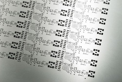
A PCB stencil, also called a solder stencil or solder paste stencil, is a thin sheet with precisely cut openings used to deposit solder paste onto the surface-mount pads of a printed circuit board. During PCB assembly, the stencil controls where solder paste is printed and, just as importantly, how much paste is deposited.
That makes stencil design an important part of the surface mount technology (SMT) assembly process. Too little solder paste can contribute to insufficient solder joints or opens. Too much can increase the risk of bridging, solder balls, component movement, and other assembly defects.
A well-designed PCB stencil considers component pitch, pad geometry, aperture dimensions, stencil thickness, solder paste characteristics, and the assembly process together. For boards containing fine-pitch components, BGAs, QFNs, or very small passives, these decisions become even more important.
What Is a PCB Stencil?
A PCB stencil is typically a thin metal foil containing openings, called apertures, that correspond to selected surface-mount pads on a PCB.
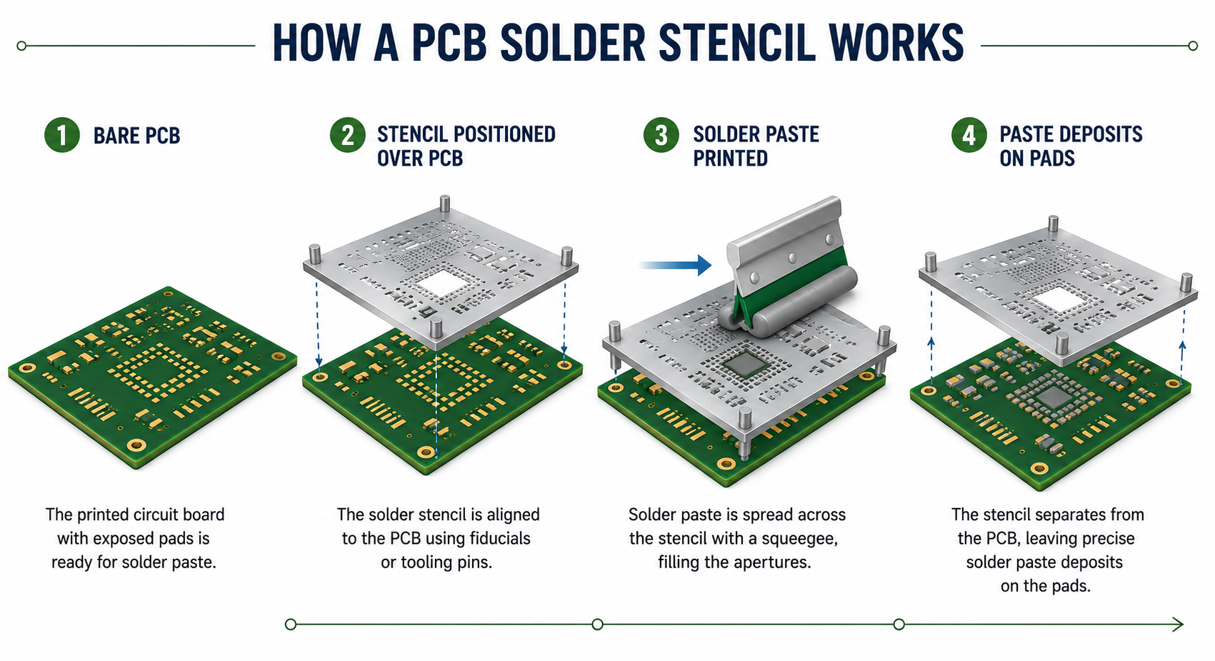
During solder paste printing, the stencil is aligned over the board. Solder paste is moved across the stencil with a squeegee, filling the apertures. When the stencil separates from the PCB, the paste should release cleanly and remain on the pads.
Components are then placed into the printed solder paste before the assembly enters the reflow oven. The basic process is:
Align stencil → Apply solder paste → Print through apertures → Separate stencil → Place components → Reflow
Although the process appears simple, solder paste printing is sensitive to several interacting variables. Stencil thickness, aperture geometry, paste properties, board support, squeegee parameters, alignment, and stencil release can all influence the quality of the print.
Why Is a PCB Stencil Important?
The stencil controls solder paste volume across the PCB. That matters because modern circuit boards often combine very different component types. A single assembly might contain large connectors, QFNs, BGAs, fine-pitch ICs, and tiny passive components. Each may have different solder paste requirements. For example, a large component termination may require more solder volume than a small fine-pitch pad. Simply making every stencil opening identical to the corresponding PCB pad does not always produce the best result.
A properly engineered solder stencil can help:
- Control solder paste volume
- Improve print repeatability
- Reduce solder bridging
- Reduce insufficient solder deposits
- Improve fine-pitch printing
- Control paste beneath bottom-terminated components
- Improve first-pass assembly yield
Stencil design therefore needs to be considered as part of the assembly process rather than as a simple copy of the PCB paste layer.
How Is a PCB Stencil Made?
SMT stencils are commonly manufactured from stainless-steel foil using laser cutting. The laser creates the individual apertures according to the stencil data. Aperture size and geometry can be modified from the original pad dimensions when the assembly process requires a different solder paste deposit. AdvancedPCB's existing stencil offering uses laser-cut Type 304 stainless steel.
After cutting, stencil manufacturing processes may include additional finishing or treatment designed to improve aperture quality and paste release. The exact manufacturing method and treatment depend on the stencil supplier and application. Stencil accuracy becomes increasingly important as component pitch and aperture dimensions decrease.
PCB Stencil Thickness
Stencil thickness is one of the primary factors controlling solder paste volume. A thicker stencil generally deposits more paste through a given aperture. A thinner stencil generally deposits less paste and may provide better release for very small apertures.
There is no single correct thickness for every PCB.
IPC technical literature notes that fine-pitch components may require thinner foils, while larger components and some through-hole paste applications may require thicker deposits.
The appropriate stencil thickness depends on factors such as:
- Smallest component and pad geometry
- Component pitch
- Required solder volume
- Aperture dimensions
- Solder paste characteristics
- Board design
- Printing equipment
- Mix of component sizes
This creates a common design challenge: a board may contain small components that favor a thin stencil and larger components that need more paste.
PCB Stencil Aperture Design
An aperture is the opening through which solder paste is printed. Aperture geometry directly affects the amount of paste deposited and how easily it releases from the stencil. In some locations, a stencil aperture may closely follow the PCB land geometry. In others, the opening may be reduced, enlarged, divided, or reshaped to control paste deposition. Examples include:
Fine-pitch components: Apertures may be adjusted to reduce bridging while maintaining sufficient solder volume.
QFNs and other bottom-terminated components: The large center thermal pad often uses multiple smaller stencil openings rather than one large opening. This helps control paste volume and can influence solder behavior during reflow.
Small passive components: Aperture geometry can be adjusted to improve paste transfer and help manage solder-related defects.
Pin-in-paste applications: Selected through-hole locations may require additional paste volume to achieve the required solder joint.
There is no universal aperture reduction that works for every assembly. Component geometry, stencil thickness, paste, pad design, and process capability should determine the aperture design.
Area Ratio and Solder Paste Release
One of the most useful concepts in solder stencil design is area ratio. IPC-7525 defines area ratio as the area of the aperture opening divided by the area of the aperture walls.
As apertures become smaller relative to stencil thickness, solder paste has more wall area to interact with compared with the size of the opening. Paste may then have difficulty releasing cleanly from the aperture.
This becomes especially important with fine-pitch components and very small passive devices.
An area ratio around 0.66 or greater has traditionally been used as a common starting guideline for stencil design, although actual print performance depends on stencil technology, solder paste, aperture geometry, printer settings, and other process variables. IPC technical literature discusses this 0.66 guideline while emphasizing that printing performance depends on multiple factors. For very small apertures, the stencil and assembly supplier should evaluate the actual process rather than relying on one ratio alone.
Framed vs. Frameless PCB Stencils
PCB stencils can be supplied in different configurations depending on how they will be used.
- Framed stencils permanently mount the foil within a frame and tensioning system. They are commonly used with automated stencil printers where consistent foil tension and alignment are important.
- Frameless stencils use a removable foil designed for a compatible tensioning frame. They can reduce storage requirements and may be useful in environments that process many different assemblies.
For prototypes and manual assembly, simpler stencil configurations may also be appropriate.
The right choice depends on production volume, printing equipment, changeover frequency, storage, and the required level of process control.
PCB Stencils for Fine-Pitch Components
As components become smaller, stencil design becomes more demanding.
Fine-pitch BGAs, QFNs, chip-scale packages, and small passive components reduce the available aperture dimensions. That can make consistent solder paste transfer more difficult.
Engineers should consider:
- Aperture area ratio
- Stencil thickness
- Paste particle size
- Aperture geometry
- Pad dimensions
- Solder mask design
- Stencil-to-board alignment
- Board support during printing
For BGA applications specifically, IPC-7095 provides design and assembly guidance for BGA and fine-pitch BGA technology. IPC currently lists IPC-7095E, released in 2024, as the current revision.
Fine-pitch designs should be reviewed with the assembler before stencil fabrication whenever possible.
IPC Standards for PCB Stencils and Solder Paste Printing
Several IPC documents are particularly relevant to solder stencil design and SMT printing.
IPC-7525C, Stencil Design Guidelines
Provides guidance for stencil design and fabrication, including apertures, stencil technologies, step stencils, and other design considerations. IPC lists Revision C, released in November 2021, as the current revision.
IPC-7527, Requirements for Solder Paste Printing
Addresses requirements associated with the solder paste printing process.
IPC J-STD-005B, Requirements for Solder Pastes
Establishes requirements and test methods for solder paste. Revision B was released in 2024.
IPC J-STD-001J, Requirements for Soldered Electrical and Electronic Assemblies
Addresses materials and process requirements for producing soldered electronic assemblies.
IPC-A-610J, Acceptability of Electronic Assemblies
Provides post-assembly acceptance criteria and is commonly used alongside J-STD-001.
These standards serve different purposes. IPC-7525 is the most directly applicable reference for solder stencil design.
Common PCB Stencil Problems
Many soldering defects that appear after reflow can begin during the solder paste printing process. Common issues include:
| Problem | Possible Stencil-Related Cause |
|---|---|
| Insufficient solder | Poor paste release, undersized aperture, inappropriate stencil thickness |
| Solder bridging | Excess paste, aperture geometry, or print misalignment |
| Inconsistent deposits | Clogged apertures, poor board support, print-process variation |
| Paste smearing | Poor stencil separation, alignment, or underside contamination |
| Component solder imbalance | Uneven paste volume between component terminations |
| Excessive QFN center-pad solder | Too much paste deposited beneath the thermal pad |
Not every solder defect is caused by the stencil. Component solderability, PCB finish, land pattern, solder paste, placement, reflow profile, and board design can also contribute.
That distinction matters during root-cause analysis.
What Information Is Needed to Order a PCB Stencil?
At minimum, stencil fabrication requires accurate paste-layer data and identification of the PCB or assembly revision.
Depending on the application, additional information may include:
- PCB dimensions
- Panel or array configuration
- Stencil thickness
- Frame requirements
- Component or aperture modifications
- Fiducial requirements
- Step-up or step-down regions
- Special paste-volume requirements
- Board-side relief requirements
The stencil data should match the exact revision being assembled. Using an outdated stencil after a PCB or component footprint revision can create solder paste deposits that no longer match the board.
For complex assemblies, stencil design should be reviewed as part of Design for Assembly (DFA) before production begins.
Choosing the Right PCB Stencil
A good PCB stencil does more than put solder paste on a board. It helps deliver the correct volume of paste to thousands of individual solder joints in a repeatable manufacturing process. Start with the component mix and PCB land patterns. Then consider stencil thickness, aperture dimensions, area ratio, solder paste, and printing equipment together. For straightforward assemblies, a standard laser-cut stainless-steel stencil may be sufficient. Fine-pitch devices, mixed component technologies, bottom-terminated components, or unusual solder-volume requirements may require aperture modifications or a stepped stencil.
The best time to address these requirements is before assembly starts. A stencil review during DFA can identify potential printing problems before they become soldering defects on the production floor.
FAQs for PCB stencil
Related Posts

Built for the Factory Floor

Is Your Robotic PCB Design Ready for Manufacturing?