


The PCB Fabrication Process
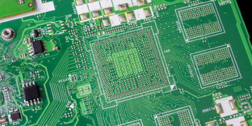
PCB fabrication is the manufacturing process used to transform digital design files into bare printed circuit boards. The process combines precision imaging, chemical processing, drilling, copper plating, lamination, inspection, and electrical testing to create reliable circuit boards for products ranging from consumer electronics and medical devices to aerospace, defense, telecommunications, and AI infrastructure.
Although the exact process varies depending on board complexity, nearly every multilayer PCB follows the same core manufacturing workflow: front-end engineering, inner-layer fabrication, lamination, drilling, copper plating, outer-layer imaging, solder mask application, surface finishing, electrical testing, and final inspection.
Understanding these steps helps engineers design boards that are easier to manufacture, improve yields, reduce production delays, and accelerate time to market. Whether you're designing a prototype, sourcing production boards, or learning how electronics are manufactured, understanding the PCB fabrication process helps engineers improve manufacturability, reduce production delays, and make better design decisions. This guide explains the complete PCB fabrication process step by step, showing how a bare circuit board is manufactured from design files through final inspection and shipment.
PCB Fabrication Process at a Glance
Printed circuit board fabrication follows a highly controlled manufacturing process that transforms digital design files into finished bare circuit boards ready for electronic assembly. While the exact process varies depending on board complexity, materials, and performance requirements, most multilayer PCBs follow the same core manufacturing workflow.
- Front-End Engineering. Manufacturing data is reviewed, design-for-manufacturability (DFM) checks are performed, and tooling files are prepared to ensure the design can be built reliably and efficiently.
- Inner-Layer Fabrication. Copper-clad laminate cores are cleaned, imaged, etched, and inspected to create the internal signal and power layers that will become part of the finished board.
- Layer Stack-Up and Lamination. Inner layers, prepreg, and copper foil are precisely aligned and bonded together under heat and pressure to form a single multilayer PCB.
- Drilling. Mechanical drills and laser systems create through-holes, blind vias, buried vias, and microvias that will provide electrical connections between layers.
- Hole Preparation and Copper Deposition. Drilled holes are cleaned and desmeared before electroless copper creates a conductive seed layer, allowing subsequent electrolytic copper plating.
- Outer-Layer Imaging and Pattern Plating. The outer circuit layers are imaged, plated, and etched to form the finished copper traces, pads, and plated through-holes.
- Solder Mask, Silkscreen, and Surface Finish. Protective solder mask is applied, component markings are printed, and a surface finish such as ENIG or HASL is added to preserve solderability and protect exposed copper.
- Electrical Testing and Inspection. Finished boards undergo electrical testing, automated optical inspection (AOI), dimensional verification, and visual inspection to confirm they meet design and quality requirements.
- Packaging and Shipment. Completed boards are packaged using ESD-safe materials, moisture protection, and traceability documentation before being shipped for assembly or final product integration.
.png "01-process-flow-(1).png")
Typical PCB Fabrication Overall Lead Time
Although every PCB is different, the timeline below shows the typical sequence of manufacturing steps from front-end engineering through final shipment.
| Board Type | Typical Lead Time* |
|---|---|
| Standard 2-4 Layer PCB | 3-5 Business Days |
| Quick-Turn Prototype | 24-72 Hours |
| Multilayer PCB | 5-15 Business Days |
| HDI PCB | 1-3 Weeks |
| Rigid-Flex PCB | 2-4 Weeks |
* Actual manufacturing time varies based on board complexity, material availability, production volume, and required testing.
1. PCB Manufacturing Begins with Front-End Engineering
From there, manufacturing engineers review the design against customer requirements and applicable IPC standards before creating a fabrication traveler, the master instruction sheet that follows the job through every stage of production. The traveler defines the PCB stack-up, materials, panel configuration, inspection requirements, and manufacturing process needed to build the board consistently and according to specification.
Boards are rarely manufactured individually. Instead, multiple PCBs are typically arranged into a production panel to maximize material utilization, improve manufacturing efficiency, and simplify handling throughout fabrication. Depending on the design, panelization may be provided by the customer or optimized by the PCB manufacturer.
Next comes CAM (Computer-Aided Manufacturing) engineering and Design for Manufacturability (DFM) analysis. During this critical review, engineers verify that the design can be manufactured reliably by checking trace widths and spacing, annular rings, drill sizes, solder mask clearances, copper-to-edge spacing, controlled impedance requirements, and other fabrication rules. The design netlist may also be compared against the manufacturing database to identify potential connectivity issues before production begins.
CAM engineers then generate all of the manufacturing tooling required downstream, including Laser Direct Imaging (LDI) files, CNC drilling and routing programs, electrical test data, solder mask and legend artwork, along with production features such as fiducials, tooling holes, test coupons, copper balancing, and other process aids that improve registration, plating uniformity, and overall manufacturing quality.
By identifying manufacturability issues before fabrication begins, front-end engineering helps reduce production delays, improve yields, minimize costly redesigns, and ensure the PCB can move efficiently from digital design files to finished bare circuit boards ready for assembly.
2. How Inner PCB Layers Are Manufactured
For multilayer printed circuit boards, the inner layers are fabricated first because they will eventually become permanently embedded within the finished PCB. At this stage, the copper circuitry that carries signals and distributes power is created on individual laminate cores before the board is assembled into a multilayer stack.
-
Surface Preparation. Each copper-clad laminate core is thoroughly cleaned using a combination of mechanical brushing, pumice scrubbing, and chemical cleaning to remove oxidation, fingerprints, oils, and other surface contaminants. Proper surface preparation is critical because even microscopic contamination can reduce photoresist adhesion, affect etching accuracy, or create defects that impact long-term reliability.
-
Photoresist Lamination. After cleaning, a light-sensitive dry-film photoresist, typically between 0.0013 and 0.002 inch thick, is laminated onto both sides of the copper-clad core using heated rollers. A protective polyester film remains on the outer surface until imaging to prevent contamination and protect the photoresist during handling.
-
Laser Direct Imaging (LDI). Rather than using traditional phototools, most modern PCB manufacturers use Laser Direct Imaging (LDI) systems to expose the circuit pattern directly onto the photoresist inside a cleanroom environment. LDI improves image accuracy, eliminates film distortion, and provides layer-to-layer registration typically within approximately 20 to 25 μm (about ±0.001 inch), making it well suited for today's fine-line and high-density PCB designs. At this stage, the CAM-generated manufacturing data is transferred into a precise physical circuit pattern.
-
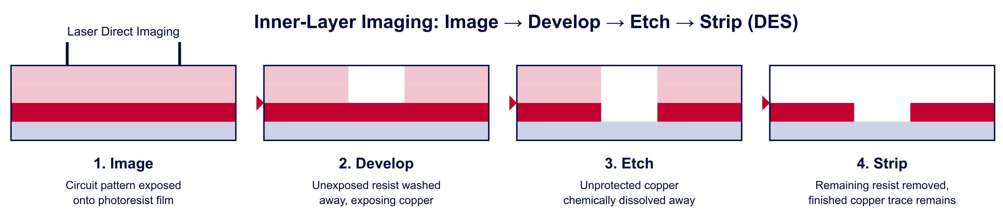
Develop, Etch, and Strip (DES). The imaged panels then pass through a conveyorized Develop-Etch-Strip (DES) process. During development, the unexposed photoresist is removed to reveal the copper that will be etched away. Chemical etching dissolves the unwanted copper while leaving the protected circuit pattern intact. Finally, the remaining photoresist is stripped away, exposing the completed copper traces and plane features that form the finished inner-layer circuitry.
.png "03-des-process-(1).png")
-
Automated Optical Inspection (AOI). Each completed inner layer undergoes Automated Optical Inspection (AOI) before moving to lamination. AOI systems align the panel using registration fiducials and perform a pixel-by-pixel comparison against the original manufacturing data to detect opens, shorts, nicks, under-etching, over-etching, missing copper, or other pattern defects. Identifying these issues before the layers are laminated together significantly improves manufacturing yields, reduces scrap, and prevents defects from becoming permanently embedded inside the finished PCB.
3. How PCB Layers Are Laminated Together
After the inner layers have been fabricated and inspected, they are combined into a single multilayer printed circuit board through the lay-up and lamination process. This stage permanently bonds the individual copper-clad cores, prepreg, and outer-layer copper foil into one solid structure that provides both mechanical strength and electrical integrity.
Before lay-up begins, each inner-layer core undergoes an oxide or oxide-alternative treatment that chemically prepares the copper surface for bonding. This treatment creates a microscopically roughened surface that improves adhesion between the copper and the prepreg resin, helping ensure long-term reliability during thermal cycling and normal operating conditions.
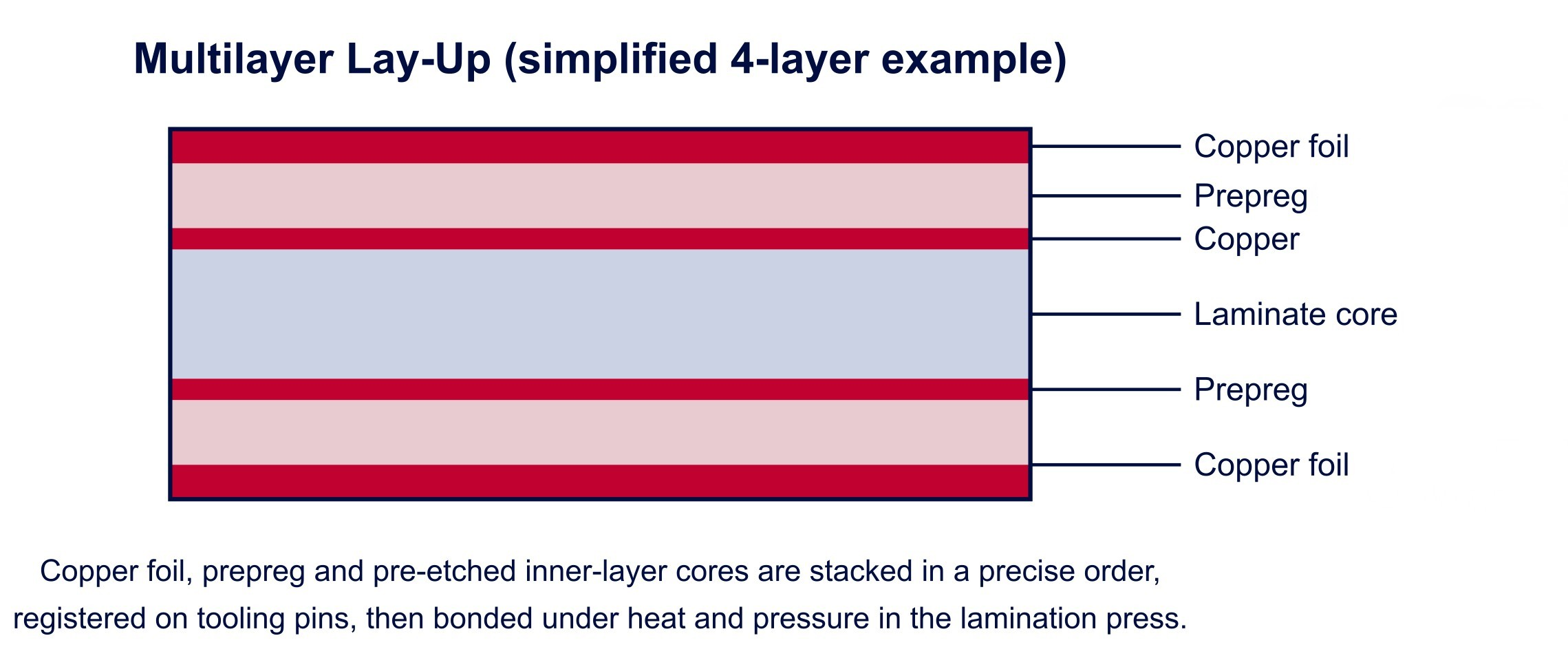
Following the fabrication traveler, manufacturing technicians carefully stack the inner-layer cores, prepreg sheets (partially cured fiberglass-reinforced epoxy resin), and outer-layer copper foil in the precise order defined by the PCB stack-up. Tooling pins and optical registration systems are used to accurately align every layer so drilled holes and electrical features remain properly positioned throughout the finished board.
Once assembled, multiple panel stacks are placed between stainless steel separator plates to form a press "book." These books are loaded into a hydraulic lamination press where precisely controlled heat and pressure, and in many cases vacuum assist, cure the prepreg resin while eliminating trapped air and volatile gases. As the resin flows and fully cures, it permanently bonds every layer into a rigid, unified PCB structure.
After lamination is complete, the panels are cooled under controlled conditions to minimize material movement and maintain dimensional stability. Excess resin, known as flash, is removed from the panel edges, leaving a clean laminated panel with all inner-layer circuitry permanently encapsulated and ready for the drilling process.
Because the entire multilayer PCB depends on proper layer registration and bond integrity, the lay-up and lamination process is one of the most critical stages of PCB fabrication. Precise control of materials, temperature, pressure, and alignment helps ensure reliable electrical performance while minimizing the risk of delamination, layer misregistration, and other manufacturing defects.
.png "Untitled-design-(14).png")
4. How Holes and Vias Are Drilled in a PCB
After the multilayer PCB has been laminated into a single panel, holes are drilled to create the electrical pathways that will connect copper layers throughout the board. Depending on the PCB design, manufacturers use both mechanical drilling and laser drilling to produce through-holes, blind vias, buried vias, and microvias with the precision required for modern electronic assemblies.
-
Mechanical Drilling. Mechanical drilling uses high-speed CNC drilling machines equipped with solid carbide drill bits to produce plated through-holes and other larger hole features. Drill diameters typically range from approximately 0.0059 to 0.200 inches, depending on the application and board thickness. These holes may be used for component leads, mounting hardware, tooling, or electrical interconnections between all layers of the PCB.
Because the internal circuitry is no longer visible after lamination, precise registration is essential. Fabricators commonly use X-ray registration systems to locate internal layer targets before drilling begins, ensuring the holes align accurately with buried copper pads and maintain the required annular ring specified by the design. -
Laser Drilling. Laser drilling is primarily used to produce microvias for High-Density Interconnect (HDI) circuit boards. Unlike mechanically drilled through-holes, microvias typically connect only the outer layer to one or more adjacent layers, allowing designers to achieve higher routing density in compact electronic devices.
Different laser technologies are used depending on the materials being drilled. CO₂ lasers efficiently remove dielectric materials such as epoxy resin and fiberglass but cannot directly drill copper because it reflects infrared energy. UV lasers can machine both copper and dielectric materials with excellent precision, although at slower speeds. Many advanced PCB manufacturers combine both technologies, using a UV laser to remove the copper surface before a CO₂ laser completes the dielectric portion of the microvia. -
Precision Drilling Supports Reliable PCB Performance. Hole quality is critical because every drilled feature must later be cleaned, plated, and electrically connected. Accurate drilling minimizes positional error, maintains proper annular ring dimensions, and helps ensure reliable copper plating during subsequent manufacturing steps. As PCB designs continue to increase in layer count and density, precise drilling technology has become essential for producing reliable multilayer, HDI, and advanced packaging circuit boards.
5. How PCB Vias Become Electrically Conductive
Once drilling is complete, the holes are simply openings in fiberglass and copper. To create electrical connections between layers, the hole walls must be cleaned, prepared, and plated with copper. This process transforms drilled holes into conductive vias that carry electrical signals and power throughout the finished PCB.
-
Deburring and Desmearing. The first step is removing any drilling residue that could interfere with copper adhesion. Mechanical brushing removes burrs left on the copper surface, while chemical or plasma desmear processes eliminate epoxy resin that can smear across the exposed internal copper during drilling. Removing this resin is essential because it would otherwise insulate the internal copper layers and prevent reliable electrical connections.
-
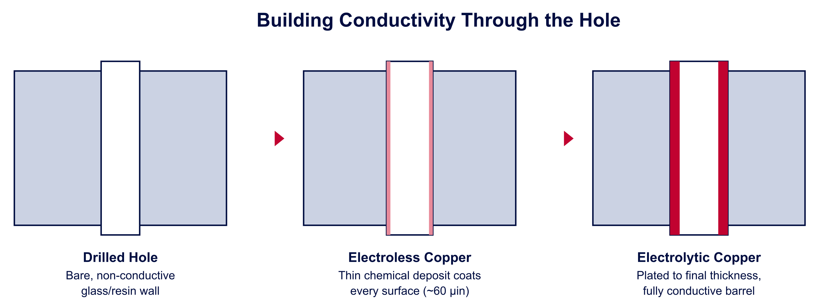
Electroless Copper Deposition. After cleaning, the panels undergo electroless copper deposition. Unlike electroplating, this chemical process does not use electrical current. Instead, it deposits a thin, uniform layer of copper over every exposed surface, including the hole walls, fiberglass, resin, and existing copper.
The electroless copper layer is typically 30 to 60 microinches thick. Although too thin to provide the required electrical performance on its own, it creates a continuous conductive surface that allows the panel to move into the electrolytic copper plating process. -
Preparing for Copper Build-Up. Once the electroless copper has been applied, every drilled hole has a conductive foundation. During the next stage of fabrication, electrolytic copper plating builds additional copper thickness inside the hole barrels and on the panel surface until the required electrical and mechanical specifications are achieved.
Reliable hole preparation is critical because defects introduced at this stage can lead to poor plating adhesion, voids, insufficient copper thickness, or long-term reliability issues. Proper cleaning and copper deposition ensure that plated through-holes and vias provide durable electrical connections capable of withstanding thermal cycling and the mechanical stresses of assembly and field operation.
6. How Outer PCB Layers Are Plated and Etched
With the drilled holes now electrically conductive, the outer layers of the PCB can be formed. This stage creates the final copper circuitry on the board surface while simultaneously building the copper thickness inside plated through-holes and vias to meet design and IPC requirements.
-
Outer-Layer Imaging. The outer copper surfaces are first cleaned and laminated with a light-sensitive photoresist, much like the inner-layer fabrication process. Using Laser Direct Imaging (LDI), the outer-layer circuit pattern is exposed onto the photoresist with high precision. After development, only the areas where additional copper is required remain exposed.
Unlike the inner layers, where unwanted copper is removed, the outer-layer process uses a pattern plating approach that adds copper only where the finished circuits and plated holes will be located. -
Electrolytic Copper Plating. The panels are immersed in an electrolytic copper plating bath, where electrical current deposits copper onto the exposed conductive surfaces. This process simultaneously increases the copper thickness inside the plated through-holes and vias while building the finished copper traces, pads, and planes on the outer layers.
Carefully controlled plating chemistry, current density, solution agitation, and process time help ensure uniform copper thickness across the panel and within the hole barrels. Consistent plating is essential for electrical reliability, solderability, and compliance with IPC performance requirements. -
Tin Plating and Pattern Etching. After copper plating, a thin layer of tin is plated over the newly deposited copper. The tin serves as a temporary etch resist that protects the finished circuit pattern during the subsequent etching process.
The remaining photoresist is stripped away, exposing the unwanted background copper. Chemical etching removes this excess copper while the tin protects the finished traces beneath it. Once etching is complete, the temporary tin layer is chemically removed, leaving the completed outer-layer copper circuitry fully exposed and ready for solder mask application. -
Creating the Finished Outer Circuitry. Outer-layer imaging, copper plating, and pattern etching work together to produce the finished conductive features that connect electronic components across the PCB. Precise process control throughout these operations helps maintain trace geometry, copper thickness, and via reliability, ensuring the circuit board meets its electrical performance and long-term reliability requirements before moving to the final finishing processes.
7. Applying Solder Mask, Silkscreen, and Surface Finish
After the outer-layer circuitry has been completed, the PCB enters the finishing stage. During this phase, solder mask, silkscreen, and a surface finish are applied to protect the exposed copper, improve solderability, and prepare the bare board for component assembly.
-
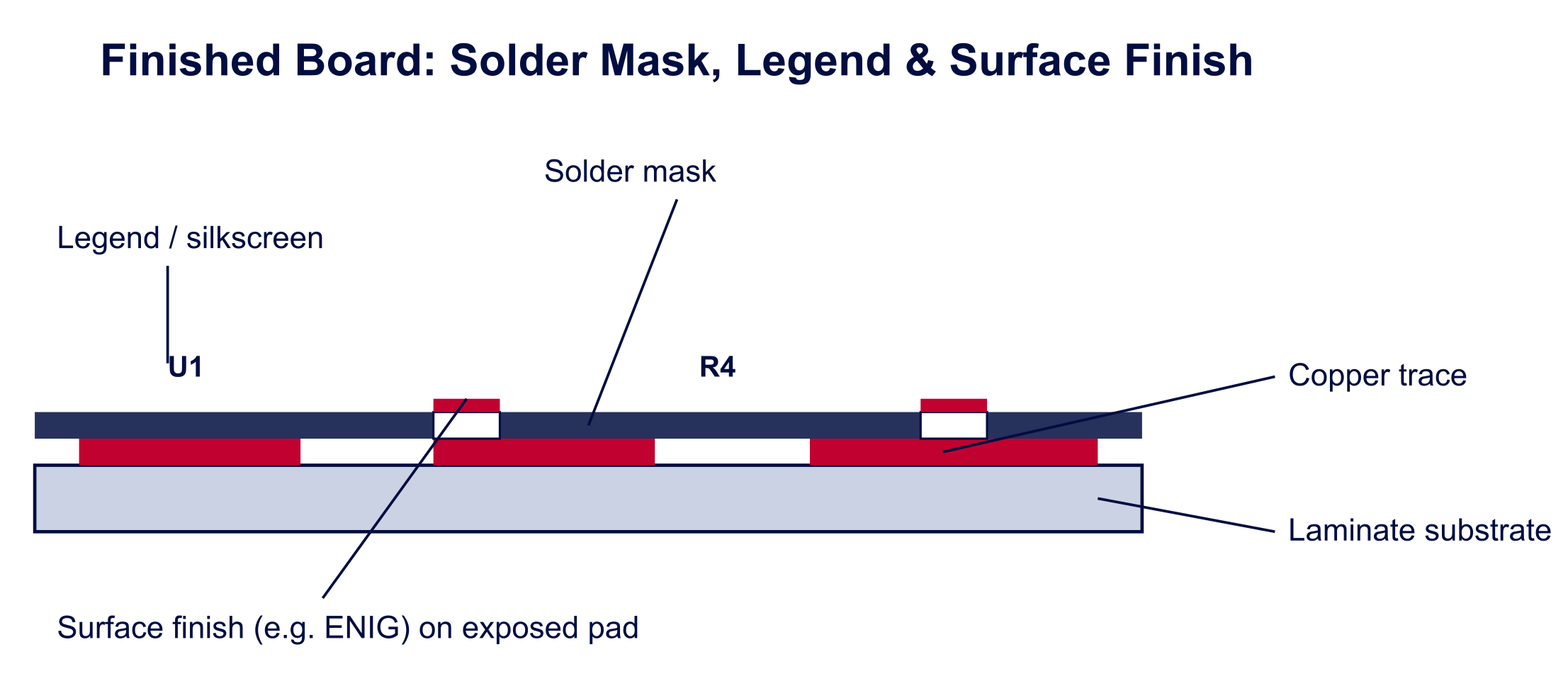
Solder Mask Application. The first step is applying solder mask, a durable polymer coating that covers nearly all exposed copper except the pads and other areas intended for soldering. Most manufacturers use Liquid Photoimageable (LPI) solder mask because it provides excellent adhesion, precise feature definition, and compatibility with fine-pitch surface-mount components.
The solder mask is applied across the panel, exposed using imaging equipment, developed to remove material from the solderable areas, and then fully cured. Besides preventing unwanted solder bridges during assembly, solder mask protects the copper circuitry from oxidation, moisture, chemicals, and mechanical damage throughout the product's operating life. - Silkscreen (Legend) Printing. After the solder mask has cured, the PCB legend, commonly called the silkscreen, is added. Modern manufacturers typically use UV inkjet printing to apply reference designators, component outlines, polarity markings, company logos, revision identifiers, and other assembly information directly onto the board surface. Although the silkscreen does not affect the PCB's electrical performance, it plays an important role during assembly, inspection, testing, troubleshooting, and field repair by helping technicians accurately identify component locations and board orientation.
-
Surface Finish. The final manufacturing step before testing is applying a surface finish to the exposed copper pads. Surface finishes protect the copper from oxidation while maintaining solderability until components are assembled.
Several surface finishes are commonly used depending on the application, including:-
Electroless Nickel Immersion Gold (ENIG)
-
Hot Air Solder Leveling (HASL)
-
Immersion Silver
-
Electroless Nickel Electroless Palladium Immersion Gold (ENEPIG)
-
ENIG is one of the most widely specified finishes for modern electronics because it provides a flat, highly solderable surface that performs well with fine-pitch surface-mount technology (SMT), ball grid array (BGA) packages, and controlled solder joints. The selection of a surface finish depends on factors such as assembly process, product reliability requirements, shelf life, cost, and environmental conditions.
-
-
Preparing the PCB for Assembly. Once the solder mask, legend, and surface finish have been applied, the bare PCB has all of the protective coatings and identification markings required for electronic assembly. The board is now ready to undergo electrical testing and final quality verification before shipment.
8. How Finished PCBs Are Tested and Inspected
Before a printed circuit board leaves the manufacturing facility, it undergoes multiple inspections and electrical tests to verify that it was built according to the design data and meets the required quality standards. These final verification steps help identify manufacturing defects before assembly and improve overall product reliability.
-
Electrical Testing. Electrical testing verifies that every circuit is properly connected and isolated according to the original design netlist. Prototype and low-volume production boards are commonly tested using flying-probe systems, which move precision probes across the PCB without requiring dedicated tooling.
-
Bed-of-Nails. For higher production volumes, manufacturers often use bed-of-nails test fixtures. These custom fixtures contact hundreds or even thousands of test points simultaneously, allowing electrical verification to be completed quickly and efficiently during production. Both testing methods check for opens, shorts, and incorrect electrical connections before the boards are shipped.
-
Impedance Verification. For high-speed digital, RF, and microwave circuit boards, controlled impedance testing is often performed using test coupons fabricated alongside the production panels. These measurements verify that transmission lines meet the specified impedance values required for reliable signal integrity.
-
Profiling and Depanelization. After testing, the individual PCBs are separated from the manufacturing panel. Depending on the design, manufacturers use CNC routing, V-scoring, tab routing, or a combination of depanelization methods to produce the finished board dimensions while minimizing mechanical stress.
-
Final Inspection. Every PCB then undergoes a comprehensive final inspection. Inspectors verify board dimensions, hole sizes, surface finish quality, solder mask registration, silkscreen accuracy, edge quality, and overall workmanship. Higher-reliability products may also require additional quality verification such as microsection analysis, solderability testing, dimensional measurements, or other inspections specified by IPC standards or customer requirements.
9. Packaging and Shipment
Once the PCB passes all inspections, it is packaged to protect it during storage and transportation. Most bare boards are sealed in electrostatic discharge (ESD)-safe moisture-barrier bags with desiccant packs and humidity indicator cards to help prevent moisture absorption and electrostatic damage before assembly.
Comprehensive testing and inspection are the final safeguards in the PCB fabrication process, helping ensure every board meets the required electrical, mechanical, and quality specifications before it reaches the customer.
PCB Fabrication Process Summary
Although every printed circuit board is unique, nearly every multilayer PCB follows the same core manufacturing workflow. Front-end engineering, inner-layer fabrication, lamination, drilling, copper plating, outer-layer imaging, solder mask application, surface finishing, testing, and inspection all work together to produce reliable circuit boards that meet demanding electrical and mechanical requirements. Understanding each stage helps engineers design more manufacturable PCBs, improve yields, and accelerate product development.
Related Posts
.jpg?resizemode=force&maxsidesize=1226 "Large-Scale PCB Production")