Microvia

Our Capabilities Include Laser-Drilled Microvias
AdvancedPCB offers printed circuit board manufacturing services for the simplest prototypes to the most advanced PCBs for critical applications and high-volume production. Over the years we have made a significant capital investment in the latest equipment at our three state-of-the-art facilities to provide customers the highest quality and advanced PCB technology such as laser drilled Microvias and much more.
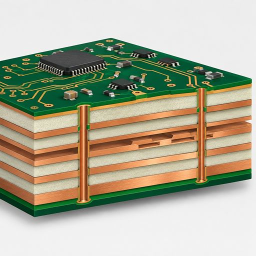
Our capabilities include Microvias, Stacked Microvias, Blind Vias, Buried Vias, Laser Direct Imaging (LDI), Via-in-Pad, up to 40 layer boards, buried chip resistors, cavity boards, multilayer RF designs, and more.
What is a Microvia?
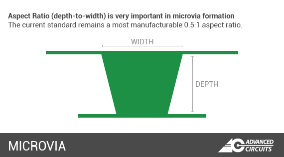
Microvias structures can be found in High Density Interconnect (HDI) printed circuit boards. These are structures being defined by the aspect ratio of a hole, which is the ratio of the length or depth of a hole to its preplated diameter. They are miniscule holes drilled by a laser in multilayer circuit boards to create the connection between layers.
IPC-2226 1.5.2 HDI Types (I, II, & III of VI)
- TYPE I: (1 + n + 1) Laser Microvias on Both Sides of the Board.
- TYPE II: (1 + n + 1) Laser Microvias on Both Sides of the Board, with Buried Vias in the Core.
- TYPE III: (2 + n + 2) Laser Microvias on Both Sides of the Board—may Have Buried Vias in the Core.
.png)
AdvancedPCB
Related Posts