Via Tenting for PCBs Available at AdvancedPCB
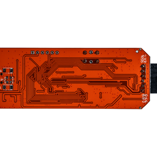
As devices get thinner and engineers use more surface mount components for their products, it is important to design and produce circuit boards with as close to absolute surface planarity as possible. Via tenting from AdvancedPCB is one of a few ways to easily prevent excess solder in via holes by covering them over with soldermask. By covering the via hole with solder mask material on the device side, the hole can be “tented†over to prevent solder from filling the hole. This effectively keeps the low profile you need for your printed circuit board.
AdvancedPCB Discusses Negatives of Via Tenting
While via tenting can be an effective way to cover the via holes on your PCB, small amounts of fluid could remain trapped in the barrel of the via hole after the soldermask is applied. This can happen during the surface finish process, for example. As such, it is best to provide a small pinhole in the tent to allow any solution to escape the hole. However, the tent/breaker option remains cost effective and does not require additional processing steps during production. Learn more by talking with an expert at AdvancedPCB today.
.png)
AdvancedPCB
Related Posts
Why Do PCBs Have an Even Number of Layers?