


What is a PCB Trace?
.jpg?resizemode=force&maxsidesize=500 "PCB Traces")
A PCB trace is a conductive copper path that carries electrical signals or power between components on a printed circuit board. Trace geometry may look simple, but it has a direct effect on electrical performance, temperature rise, voltage drop, signal integrity, manufacturability, and long-term reliability.
Choosing the right PCB trace width requires more than following a default rule in PCB design software. Current, copper thickness, layer location, temperature, voltage, impedance, manufacturing capability, and the surrounding PCB structure can all influence the final design.
This guide by AdvancedPCB's technical team explains how PCB traces work, how width and thickness affect performance, and what engineers should consider when designing traces for power and high-speed signals.
Three fundamental dimensions affect PCB trace design: width, thickness, and spacing.
Power loss = I²R
As current increases, resistive heating rises quickly. Increasing conductor cross-sectional area reduces resistance and therefore helps reduce both voltage drop and heat generation. That means current-carrying capability depends on more than PCB trace width.
Important variables include:
For high-current applications, a wide trace may not be the only solution. Designers can also use copper pours, planes, heavier copper, or multiple conductive paths when appropriate.
The DC resistance of a conductor depends primarily on:
R = ρL/A
where ρ is the resistivity of copper, L is conductor length, and A is conductor cross-sectional area.
A longer PCB trace has more resistance. Increasing width or thickness increases its cross-sectional area and reduces resistance. For power distribution, keep high-current paths reasonably short and use sufficient copper area. Evaluate both voltage drop and thermal performance rather than designing only to a current rating.
Common target impedances include 50 Ω for certain single-ended interfaces and 90 Ω or 100 Ω differential, but the correct value comes from the specific interface requirement.
Do not select a trace width from a generic online impedance calculator and assume it will produce the required finished impedance. Work with the PCB manufacturer to establish the production stackup. Actual material properties, dielectric thicknesses, copper construction, fabrication tolerances, and etching characteristics all influence the finished result.
Critical signals should generally remain referenced to an appropriate, continuous reference plane. Crossing a split or discontinuity can force return current to take a longer path, increasing loop inductance and potentially contributing to EMI or signal-integrity problems.
Other good practices include:
For many modern PCB designs, a properly manufactured 90-degree corner does not create a meaningful electrical or fabrication problem. At very high frequencies, however, changes in conductor geometry can affect impedance, so routing geometry should be evaluated as part of the transmission-line design.
45-degree bends and arcs remain common because they produce clean layouts and can simplify routing. They should not, however, be treated as a universal reliability requirement.
Current: The conductor needs sufficient cross-sectional area for the required load.
Voltage drop: Resistance along the path must not reduce voltage beyond the circuit's allowable range.
Temperature: Resistive losses should not create unacceptable conductor or board temperatures.
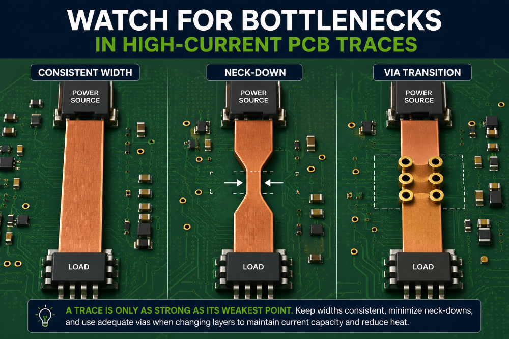
Vias: Layer transitions need sufficient conductive capacity.
Connections: Narrow neck-downs, thermal-relief spokes, connector pads, and other transitions can become bottlenecks even when the main trace is sufficiently wide.
For major power rails, copper pours or planes may provide lower resistance and better current distribution than individual traces.
The achievable trace width and spacing depend partly on copper thickness and the fabrication process. As copper becomes thicker, maintaining extremely fine trace-and-space geometry generally becomes more challenging.
Before layout, confirm the PCB manufacturer's capabilities for:
For rigid printed boards, IPC-6012F establishes qualification and performance requirements for finished boards, including single-sided, double-sided, multilayer, blind/buried via, and microvia constructions.
Undersized power traces: Narrow conductors can create excessive resistance, voltage drop, or temperature rise.
Long neck-downs: A wide power trace that narrows substantially near a pad can create a current bottleneck.
Insufficient spacing: Trace spacing may violate manufacturing capabilities, electrical requirements, or applicable safety requirements.
Poor return paths: High-speed traces routed across reference-plane discontinuities can create longer return paths and increased EMI risk.
Excessive via transitions: Unnecessary vias introduce discontinuities and can create stubs on high-speed signals.
Ignoring finished copper: Designing only around nominal starting foil can produce incorrect assumptions about final conductor geometry.
Overusing minimum features: Just because a manufacturer can produce a particular trace and space does not mean every feature should be designed at that minimum.
Power traces need sufficient copper for current, voltage drop, and thermal requirements. High-speed traces require controlled geometry and well-planned return paths. Every trace also needs to fit within the PCB manufacturer's fabrication capabilities.
The best time to resolve those requirements is before routing is complete. Establish the stackup, copper weights, impedance targets, and manufacturing rules with your PCB fabricator early. Then use calculations, simulation, and physical validation where appropriate. That approach creates PCB traces that do more than look correct in the layout. They are designed to perform reliably after the board is manufactured.
The best time to resolve those requirements is before routing is complete. Establish the stackup, copper weights, impedance targets, and manufacturing rules with your PCB fabricator early. Then use calculations, simulation, and physical validation where appropriate.
That approach creates PCB traces that do more than look correct in the layout. They are designed to perform reliably after the board is manufactured.
Choosing the right PCB trace width requires more than following a default rule in PCB design software. Current, copper thickness, layer location, temperature, voltage, impedance, manufacturing capability, and the surrounding PCB structure can all influence the final design.
This guide by AdvancedPCB's technical team explains how PCB traces work, how width and thickness affect performance, and what engineers should consider when designing traces for power and high-speed signals.
What Is a PCB Trace?
A PCB trace is a patterned copper conductor that electrically connects components and other conductive features on a printed circuit board. Instead of connecting components with individual wires, PCB traces create repeatable conductive paths directly on the board. Depending on the design, traces may carry:- Power
- Ground connections
- Low-speed digital signals
- High-speed digital signals
- Analog signals
- RF signals
PCB Trace Width, Thickness, and Spacing
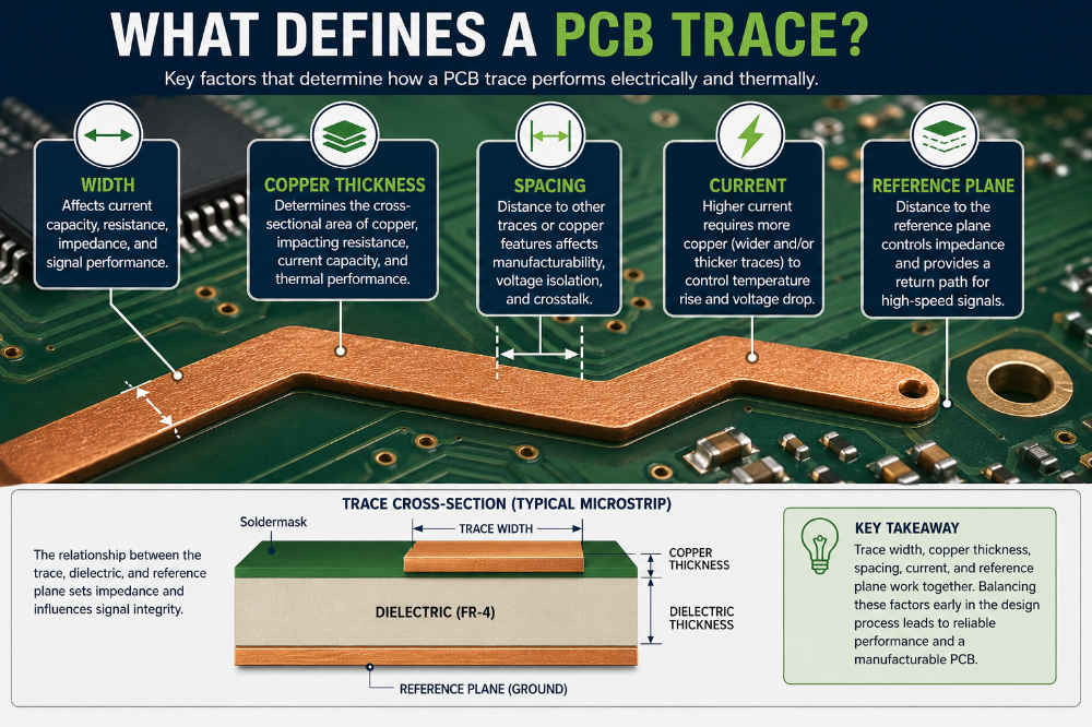
Three fundamental dimensions affect PCB trace design: width, thickness, and spacing.
PCB Trace Width
Trace width is the lateral width of the copper conductor. For a given copper thickness, increasing trace width increases conductor cross-sectional area. This reduces DC resistance and therefore reduces voltage drop and resistive heating for a given current. Signal traces may be relatively narrow when current requirements are low. Power traces often need greater width or larger copper areas. The correct width depends on the application rather than a universal PCB trace-width rule.PCB Trace Thickness
PCB trace thickness is largely determined by the copper construction and subsequent fabrication processes. Common starting copper foil weights include:- 0.5 oz/ft²: approximately 17 µm
- 1 oz/ft²: approximately 35 µm
- 2 oz/ft²: approximately 70 µm
PCB Trace Spacing
PCB trace spacing is the edge-to-edge distance between adjacent conductive features. Required spacing depends on several factors:- PCB manufacturer's process capability
- Copper thickness
- Operating voltage
- Electrical safety requirements
- Signal-integrity requirements
- Environmental conditions
- Applicable product standards
How Does PCB Trace Width Affect Current Capacity?
A PCB trace carrying electrical current generates heat because the copper has electrical resistance. The basic relationship is:Power loss = I²R
As current increases, resistive heating rises quickly. Increasing conductor cross-sectional area reduces resistance and therefore helps reduce both voltage drop and heat generation. That means current-carrying capability depends on more than PCB trace width.
Important variables include:
- Trace width
- Copper thickness
- Trace length
- Ambient temperature
- Nearby copper
- Board construction
- Layer location
- Airflow
- Allowable temperature rise
How Do You Calculate PCB Trace Width for Current?
There is no single trace-width formula that accurately describes every PCB construction. A practical design process is:- Determine the maximum continuous and peak current.
- Establish an acceptable conductor temperature rise.
- Define the copper thickness.
- Evaluate the trace within the intended PCB stackup and thermal environment.
- Check voltage drop across the conductor.
- Add appropriate engineering margin.
- Validate critical high-current designs through analysis or physical testing.
For high-current applications, a wide trace may not be the only solution. Designers can also use copper pours, planes, heavier copper, or multiple conductive paths when appropriate.
PCB Traces and Voltage Drop
Temperature rise is only one consideration for power traces. Voltage drop can become significant on long traces even when the conductor operates at an acceptable temperature.The DC resistance of a conductor depends primarily on:
R = ρL/A
where ρ is the resistivity of copper, L is conductor length, and A is conductor cross-sectional area.
A longer PCB trace has more resistance. Increasing width or thickness increases its cross-sectional area and reduces resistance. For power distribution, keep high-current paths reasonably short and use sufficient copper area. Evaluate both voltage drop and thermal performance rather than designing only to a current rating.
Using Vias on High-Current PCB Traces
A wide trace can still develop a bottleneck when current moves between layers through vias. Via current capability depends on factors such as finished hole size, copper plating, number of vias, thermal environment, and the connections to surrounding copper. For high-current layer transitions, multiple vias are commonly used to distribute current and reduce localized resistance. Avoid assuming that simply adding a large number of vias solves every current-density problem. The via field and its connection to the planes or traces need to be evaluated as part of the complete current path.
PCB Trace Design for Controlled Impedance
At sufficiently high signal speeds, a PCB trace behaves as a transmission line. Its characteristic impedance is influenced by:- Trace width
- Copper thickness
- Distance to the reference plane
- Dielectric properties
- Trace geometry
- Nearby conductive structures
Common target impedances include 50 Ω for certain single-ended interfaces and 90 Ω or 100 Ω differential, but the correct value comes from the specific interface requirement.
Do not select a trace width from a generic online impedance calculator and assume it will produce the required finished impedance. Work with the PCB manufacturer to establish the production stackup. Actual material properties, dielectric thicknesses, copper construction, fabrication tolerances, and etching characteristics all influence the finished result.
High-Speed PCB Trace Routing
High-speed trace design is about more than making traces short. The return path matters just as much.Critical signals should generally remain referenced to an appropriate, continuous reference plane. Crossing a split or discontinuity can force return current to take a longer path, increasing loop inductance and potentially contributing to EMI or signal-integrity problems.
Other good practices include:
- Minimize unnecessary via transitions.
- Maintain the required differential-pair geometry.
- Match lengths where the interface requires timing or skew control.
- Maintain appropriate spacing between aggressive and sensitive signals.
- Avoid unnecessary stubs.
- Use appropriate termination when required by the signaling interface.
- Consider via-stub reduction techniques such as backdrilling when signal speed and board construction justify them.
Do PCB Traces Need 45-Degree Corners?
Not necessarily. The traditional rule that PCB traces must always use 45-degree corners is often overstated.For many modern PCB designs, a properly manufactured 90-degree corner does not create a meaningful electrical or fabrication problem. At very high frequencies, however, changes in conductor geometry can affect impedance, so routing geometry should be evaluated as part of the transmission-line design.
45-degree bends and arcs remain common because they produce clean layouts and can simplify routing. They should not, however, be treated as a universal reliability requirement.
PCB Trace Design for Power
Power traces require a different set of priorities from many signal traces. Consider:Current: The conductor needs sufficient cross-sectional area for the required load.
Voltage drop: Resistance along the path must not reduce voltage beyond the circuit's allowable range.
Temperature: Resistive losses should not create unacceptable conductor or board temperatures.
Vias: Layer transitions need sufficient conductive capacity.
Connections: Narrow neck-downs, thermal-relief spokes, connector pads, and other transitions can become bottlenecks even when the main trace is sufficiently wide.
For major power rails, copper pours or planes may provide lower resistance and better current distribution than individual traces.
PCB Trace Design for Manufacturability
A trace geometry that works in the CAD model still has to be manufactured.The achievable trace width and spacing depend partly on copper thickness and the fabrication process. As copper becomes thicker, maintaining extremely fine trace-and-space geometry generally becomes more challenging.
Before layout, confirm the PCB manufacturer's capabilities for:
- Minimum trace width
- Minimum spacing
- Copper thickness
- Controlled impedance
- Via structures
- Annular ring
- Layer registration
- Finished board thickness
For rigid printed boards, IPC-6012F establishes qualification and performance requirements for finished boards, including single-sided, double-sided, multilayer, blind/buried via, and microvia constructions.
Common PCB Trace Design Mistakes
Several trace-design problems appear repeatedly during DFM reviews.Undersized power traces: Narrow conductors can create excessive resistance, voltage drop, or temperature rise.
Long neck-downs: A wide power trace that narrows substantially near a pad can create a current bottleneck.
Insufficient spacing: Trace spacing may violate manufacturing capabilities, electrical requirements, or applicable safety requirements.
Poor return paths: High-speed traces routed across reference-plane discontinuities can create longer return paths and increased EMI risk.
Excessive via transitions: Unnecessary vias introduce discontinuities and can create stubs on high-speed signals.
Ignoring finished copper: Designing only around nominal starting foil can produce incorrect assumptions about final conductor geometry.
Overusing minimum features: Just because a manufacturer can produce a particular trace and space does not mean every feature should be designed at that minimum.
PCB Trace Design Checklist
Before releasing the design, verify:- Trace width supports required current and acceptable temperature rise.
- Voltage drop is acceptable on critical power paths.
- Finished copper requirements are clearly defined.
- Trace and space meet the manufacturer's capabilities.
- Electrical clearances meet applicable requirements.
- Controlled-impedance traces match the agreed production stackup.
- Critical high-speed traces maintain suitable reference paths.
- Via transitions do not create current bottlenecks.
- Differential pairs meet interface-specific geometry and skew requirements.
- A DFM review has been completed.
Designing PCB Traces for Reliable Manufacturing
A well-designed PCB trace balances electrical performance with manufacturing reality.Power traces need sufficient copper for current, voltage drop, and thermal requirements. High-speed traces require controlled geometry and well-planned return paths. Every trace also needs to fit within the PCB manufacturer's fabrication capabilities.
The best time to resolve those requirements is before routing is complete. Establish the stackup, copper weights, impedance targets, and manufacturing rules with your PCB fabricator early. Then use calculations, simulation, and physical validation where appropriate. That approach creates PCB traces that do more than look correct in the layout. They are designed to perform reliably after the board is manufactured.
The best time to resolve those requirements is before routing is complete. Establish the stackup, copper weights, impedance targets, and manufacturing rules with your PCB fabricator early. Then use calculations, simulation, and physical validation where appropriate.
That approach creates PCB traces that do more than look correct in the layout. They are designed to perform reliably after the board is manufactured.
.png)
AdvancedPCB
FAQs for PCB Traces
How does PCB trace width affect impedance?
How much current can a PCB trace carry?
How wide should a PCB trace be?
What is a PCB trace?
What is the standard PCB trace thickness?
Related Posts
Heavy Copper PCBs for Automotive Electronics: Design Considerations
Explore heavy copper PCB design for automotive electronics
Heavy Copper PCBs for Automotive Electronics: Design Considerations
Read More

Built for the Factory Floor
Learn how PCB design choices support reliable performance in industrial environments.
Built for the Factory Floor
Read More

Is Your Robotic PCB Design Ready for Manufacturing?
From Working Prototype to Production-Ready Industrial Robot PCB
Is Your Robotic PCB Design Ready for Manufacturing?
Read More
Browse
All Categories
Recent Posts
View Recent Posts