


RF and Microwave PCB Services
RF and microwave PCB performance depends on precise stack-up design, material selection, and impedance control. As operating frequencies increase, dielectric stability, conductor loss, and transmission line geometry become critical to signal integrity and predictable RF performance.
AdvancedPCB manufactures RF and microwave PCBs for applications including radar, phased arrays, satellite communications, and 5G infrastructure. From quick-turn prototypes to production builds, our processes are optimized for low insertion loss, controlled impedance, and repeatable high-frequency performance.
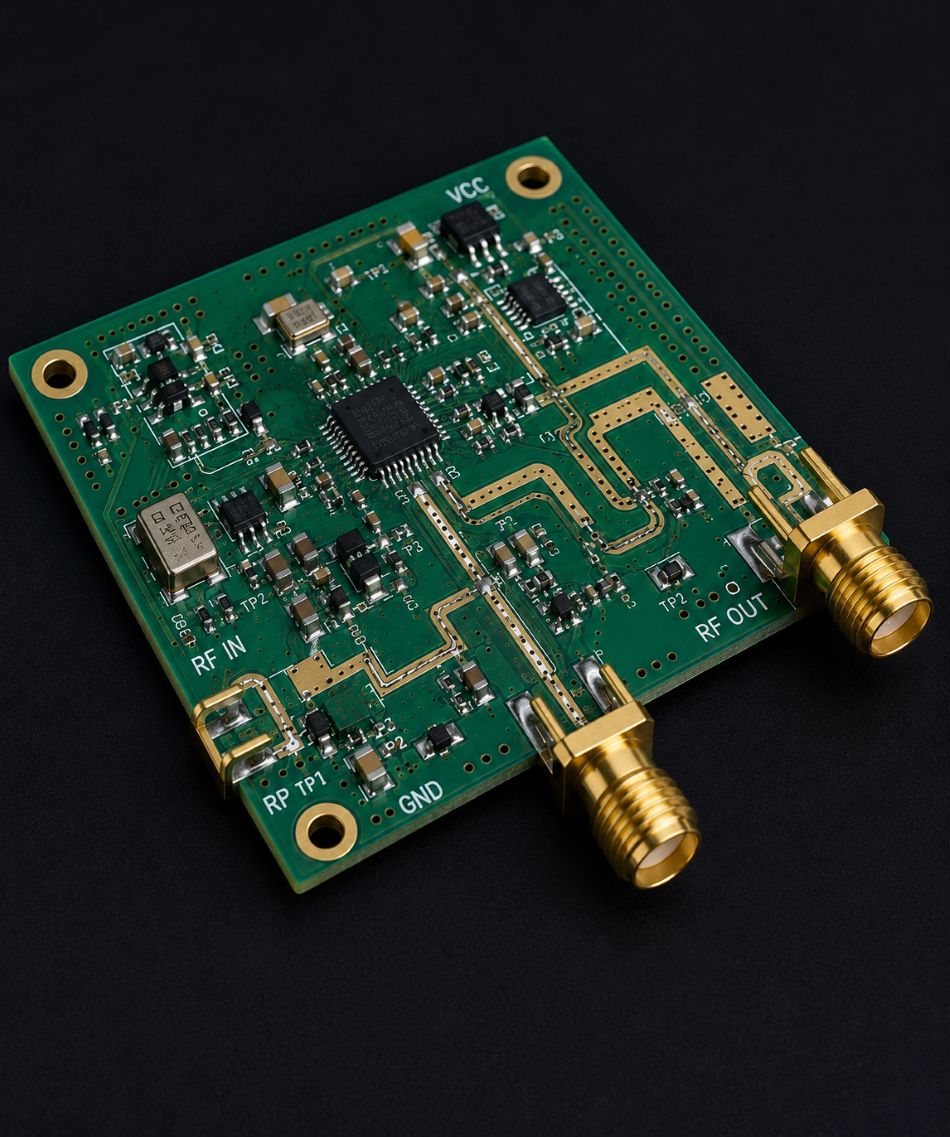
What Is an RF PCB?
An RF PCB is a printed circuit board specifically designed to carry high-frequency signals with minimal loss, reflection, or distortion. Unlike standard digital PCBs, RF and microwave designs require tighter control over dielectric properties, copper roughness, transmission line geometry, and stack-up architecture.
Key RF PCB requirements include:
- Controlled impedance structures
- Stable dielectric constant (Dk)
- Low dissipation factor (Df)
- Low conductor and dielectric loss
- Precise layer-to-layer registration
- Consistent material performance across frequency and temperature ranges
These factors directly impact insertion loss, phase stability, bandwidth, and overall RF system performance.
RF & Microwave Laminate Options
Material selection is one of the most important variables in RF PCB performance. AdvancedPCB supports a broad range of low-loss and high-frequency laminate systems for microwave and RF applications.
Supported material families include:
- Rogers RT/duroid laminates
- Rogers 4000 series materials
- Taconic RF materials
- PTFE-based laminates
- Hydrocarbon ceramic-filled materials
- Low-loss epoxy systems
| Material | Material Type | Typical DK | Typical Df | Common Applications |
|---|---|---|---|---|
| Rogers 4350B | Hydrocarbon/Ceramic | 3.66 | 0.0037 | RF modules, antennas |
| Rogers 4003C | Hydrocarbon/Ceramic | 3.55 | 0.0027 | Microwave circuits |
| RT/duroid 5880 | PTFE/Glass | 2.2 | 0.0009 | Radar and phased arrays |
| Taconic TLX | PTFE/Glass | 2.55 | 0.0012 | High-frequency RF designs |
| IS620i | Modified Epoxy | 3.58 | 0.0059 | High-speed digital/RF hybrids |
Low-profile and very-low-profile (VLP/HVLP) copper foils are often paired with these laminates to reduce conductor loss at higher frequencies.
High-Speed Hybrid Laminates
| Material | Dk | Df | Use Case |
|---|---|---|---|
| Isola Tachyon 100G | 3.02 | 0.0021 | High-speed digital layers in RF hybrid builds |
| Panasonic Megtron 7 | 3.0 | 0.002 | Backplane, high-speed compute adjacent to RF |
| Panasonic Megtron 8 | 3.1 | 0.0012 | Ultra-low-loss high-speed layers |
| AGC Meteorwave 4000 | 3.4 | 0.0019 | Cost-optimized low-loss hybrid |
| AGC Meteorwave 8000 | 3.29 | 0.0012 | High-speed RF hybrid, low loss |
| AGC Meteorwave 8300 | 3.03 | 0.0022 | mmWave-adjacent digital layers |
RF and Microwave PCB Capabilities
AdvancedPCB supports RF and microwave PCB fabrication with capabilities aligned to high-frequency and mixed-signal applications.
Capabilities include:
- RF multilayer PCBs up to eight layers
- Mixed-material stack-ups combining RF laminates and FR-4
- Fine-line capability down to 2.75 mil trace/space on suitable materials
- Controlled impedance manufacturing with standard tolerances of ±10%, with tighter tolerances available depending on stack-up and material selection
- Blind and buried vias
- Stacked microvias and HDI structures
- Backdrilling to reduce via stub effects
- Filled and capped vias for RF transitions
These capabilities help support compact RF modules, high-density interconnects, and microwave transmission structures.
If you are still debating standard vs. advanced PCB, keep in mind what you ultimately need your board to do. When you design your PCBs you can use our free DFM file check system to avoid CAM holds. You can also find a full list of capabilities online to help inform your decision.
Controlled Impedance and RF Stack-Up Design
RF stack-up architecture directly impacts insertion loss, impedance consistency, and phase stability.
AdvancedPCB works with engineers to optimize:
- Microstrip and stripline structures
- Grounded coplanar waveguide routing
- Differential pair routing
- Via transition design
- Copper foil selection and roughness
- Dielectric thickness consistency
Mixed-material RF stack-ups often combine PTFE RF layers with FR-4 or low-loss digital sections to balance electrical performance, manufacturability, and cost. These hybrid constructions require careful management of bonding compatibility, thermal expansion, and dielectric spacing during lamination.
Early stack-up collaboration helps reduce redesign cycles and improve first-pass success.
RF PCB Manufacturing Processes
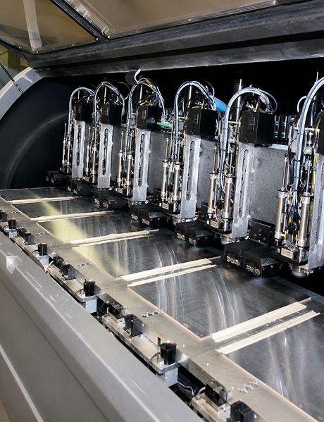
High-frequency PCB manufacturing requires tighter process control than standard PCB fabrication.
AdvancedPCB uses process controls designed to support:
- Precise etch compensation for impedance accuracy
- Laser drilling for HDI and microvia structures
- Controlled via fill and planarization
- Low-contamination processing for RF laminates
- Dedicated PTFE bake and handling procedures
- Stable dielectric spacing across multilayer constructions
Copper roughness is carefully managed to reduce conductor loss and maintain repeatable RF performance.
Design for Manufacturability: RF PCB Guidelines
Successful RF PCB fabrication begins with manufacturable layout practices.
Important RF PCB design considerations include:
- Continuous reference planes
- Controlled transmission line geometry
- Proper via antipads and backdrilling
- Ground stitching and RF isolation
- Minimized discontinuities and reflections
- Connector launch optimization
- Thermal and mechanical stability
AdvancedPCB provides engineering feedback during the design process to help align RF layout assumptions with manufacturing realities.

Applications for RF and Microwave PCBs
AdvancedPCB manufactures RF and microwave PCBs used in applications including:
- Phased array antennas
- Radar systems
- 5G and mmWave modules
- Satellite communications
- Aerospace and defense electronics
- RF instrumentation and test systems
- Wireless infrastructure
These applications require consistent RF performance, controlled loss characteristics, and reliable manufacturability.
Why Engineers Choose AdvancedPCB for RF PCB Fabrication
RF PCB manufacturing requires more than standard PCB fabrication capability. It requires process control, material expertise, and engineering collaboration focused on high-frequency performance.
Engineers choose AdvancedPCB for:
- RF-focused stack-up and material guidance
- Support for Rogers, Taconic, PTFE, and low-loss materials
- Controlled impedance manufacturing
- HDI and advanced via structures
- Quick-turn RF prototypes
- Mixed-material stack-up expertise
- U.S.-based engineering and manufacturing support
By aligning stack-up architecture, materials, and fabrication processes early, we help engineers reduce development risk and improve manufacturability before production begins. These AdvancedPCB technical guides are companion resources for engineers working through RF PCB design and manufacturing decisions
Additional RF & Microwave Design Resources
These AdvancedPCB technical guides are companion resources for engineers working through RF PCB design and manufacturing decisions.