


Is Your Robotic PCB Design Ready for Manufacturing?
An industrial robot PCB design can be electrically sound and still lack the information needed for successful manufacturing.
Industrial robot electronics may combine motor control, power conversion, processing, sensing, safety systems, and industrial communications on one board. These requirements influence the PCB stackup, materials, copper weights, routing, component placement, testing, and manufacturing documentation.
Addressing these factors before releasing the design can reduce engineering questions, manufacturing holds, redesigns, and unnecessary costs.
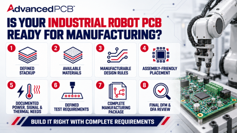
Define the PCB Stackup
The PCB stackup affects routing density, controlled impedance, power distribution, signal performance, thermal behavior, and overall board thickness.Before final routing, confirm the proposed stackup with the PCB manufacturer. The design should define:
- Layer count and layer order
- Core and prepreg materials
- Finished board thickness and tolerance
- Copper weights
- Controlled-impedance requirements
- High-current power layers
- Blind, buried, or laser-drilled vias
Design Within Manufacturing Capabilities
Routing multiple industrial robot systems into a limited board area may push trace widths, spacing, drilled holes, annular rings, or copper-to-edge clearances toward a manufacturer’s minimum limits.
The smallest feature a manufacturer can produce is not always the best choice. Designs that remain within established manufacturing capabilities are generally easier to build consistently and economically.
Advanced structures such as microvias, via-in-pad, stacked vias, and sequential lamination should be used when routing density or electrical performance justifies them. Adding complexity without a clear requirement can increase cost, lead time, and manufacturing risk.
Consider Assembly During Component Placement
Component placement affects whether the board can be assembled, inspected, tested, and repaired efficiently.
Allow sufficient clearance around connectors, BGAs, QFNs, power components, and tall parts. Confirm that automated placement and soldering processes can access each component. Parts near board edges, mounting hardware, heatsinks, or enclosures should be reviewed for mechanical interference.
Industrial robots may experience vibration, repetitive movement, abrupt stops, and cable strain. Heavy components, connectors, and mechanical interfaces may require additional support. Placement should also provide access for inspection, testing, and potential rework.
Document Power, Signals, and Thermal Requirements
Motor drives and power-conversion circuits can introduce high current, voltage transients, heat, and electrical noise. Encoders, sensors, processors, and industrial communications interfaces may depend on low-noise power and predictable signal paths.
The manufacturing documentation should clearly identify:
- Copper weight and conductor dimensions
- High-current requirements
- Voltage and clearance requirements
- Controlled-impedance targets and tolerances
- Differential-pair requirements
- Reference planes and return paths
- Grounding and shielding interfaces
- Thermal vias, copper areas, and heat-transfer paths
Build Testing Into the Design
Testability should be planned before the PCB is released. Test points, programming connections, boundary-scan access, and diagnostic interfaces can support manufacturing verification and field troubleshooting.The testing plan may include:
- Electrical testing of the bare PCB
- Automated optical inspection
- X-ray inspection for hidden solder joints
- Programming and firmware verification
- Functional testing
- Thermal testing
- Communications testing
- Mechanical-fit verification
Provide a Complete Manufacturing Package
A PCB fabrication package typically includes:
- PCB image data, such as Gerber, ODB++, or IPC-2581 files
- Plated and non-plated drill data
- Fabrication drawing
- Stackup and material requirements
- Board dimensions and tolerances
- Copper weights
- Surface finish
- Controlled-impedance specifications
- Applicable IPC class
- Electrical testing requirements
If assembly is required, the package should also include the bill of materials, approved manufacturer part numbers, pick-and-place data, assembly drawings, paste-layer data, polarity markings, programming instructions, and functional-test requirements.
All files should use matching revisions and coordinate origins. Notes on the fabrication drawing should agree with the electronic design data.
Complete DFM and DFA Reviews Before Release
Design for Manufacturability and Design for Assembly reviews can identify features that are technically possible but difficult to fabricate or assemble consistently.These reviews should evaluate the stackup, materials, trace and space, holes, vias, tolerances, solder mask, component footprints, placement clearances, panelization, test access, and manufacturing documentation.
A manufacturable industrial robot PCB must do more than meet its electrical requirements. It must also be practical to fabricate, assemble, inspect, and test at the required quality level. Involving the PCB manufacturer before the design is released helps ensure the data package is complete and the board can be built as intended.
.png)
AdvancedPCB
FAQs for Industrial Robotic Designs
Related Posts

Built for the Factory Floor

PCB Thermal Management for Robotics
.jpg?resizemode=force&maxsidesize=1226)