PCB Thermal Management for Robotics

This makes thermal management a system-level design requirement and a PCB-level reliability issue. If heat is not moved efficiently from its source to a heat sink, chassis, enclosure, or the surrounding air, component temperatures can rise, processors may throttle, electrical performance can change, and repeated thermal cycling can weaken solder joints and interconnects.
For humanoid robotics, the most effective approach is to define the thermal path early, before the PCB stackup and layout are finalized.
Thermal Management in Humanoid Robotics at a Glance
PCB designs for robotics should address six thermal priorities early:- Identify heat sources, including processors, motor drivers, power MOSFETs, regulators, converters, and battery-management electronics.
- Model steady-state loads and short, high-current events caused by walking, lifting, gripping, balancing, and recovering from motion.
- Create a continuous heat path from each source through the PCB and into a heat sink, chassis, enclosure, or other cooling structure.
- Size copper features for both current capacity and acceptable temperature rise.
- Evaluate thermal cycling, vibration, board flexure, and coefficient-of-thermal-expansion mismatches together.
- Confirm that the proposed stackup, via structures, materials, and copper weights can be manufactured consistently from prototype through production.
Why Humanoid Robots Create Difficult Thermal Conditions
A humanoid robot does not operate like a stationary computer. Loads change continuously as the machine starts, stops, balances, changes direction, and interacts with its surroundings..png "7-RIGID-FLEX-PCB-QUESTIONS-TO-ANSWER-(1).png") High-current actuator loads
High-current actuator loads
Motors and actuators can draw rapidly changing current. Current passing through traces, planes, vias, connectors, and power components creates resistive heat. Because power loss increases with the square of current, short high-current events can create disproportionate heating in undersized conductors or restricted current paths.
Dense onboard computing
CPUs, GPUs, FPGAs, memory, and high-speed communications may be located close together to reduce latency, cable length, size, and weight. Concentrating these devices also concentrates heat, creating local hot spots that must be spread across the board or transferred out of the assembly.Limited airflow and enclosure space
Electronics may be installed in the torso, head, hands, limbs, or joints. These areas can have irregular geometry, limited airflow, moving cables, and strict weight limits. A cooling method that works in a ventilated industrial cabinet may be impractical inside a humanoid robot.Repeated heating and cooling
Changing workloads cause boards and components to heat and cool repeatedly. Copper, laminate, component packages, solder, and mechanical structures expand at different rates. Over time, this thermal cycling can contribute to solder fatigue, via stress, warpage, and intermittent connections.Heat near sensitive electronics
Robotics systems combine noisy, high-power circuits with low-level sensor signals and high-speed digital interfaces. Elevated temperature can change resistance and other electrical characteristics. Poor placement or an incomplete thermal path can therefore affect power integrity, signal integrity, sensor accuracy, and control stability, not just component life.Start with the Power and Thermal Profile
Before selecting a PCB thermal-management technique, define how the robot will actually operate. Document:- Typical, peak, and fault current for each actuator group
- Duty cycles for walking, lifting, gripping, standing, and idle modes
- Expected ambient-temperature range
- Maximum component-junction and board temperatures
- Available airflow in each enclosure
- Thermal interfaces to the chassis, frame, cold plate, or heat sink
- Weight and space limits
- Expected service life and movement cycles
- Temperature, current, and processor data that can be monitored during validation
Thermal Management Techniques for PCBs
Many humanoid robotics designs use more than one thermal technique on the same board. The right combination depends on the location and intensity of the heat source, the available space, the current requirement, and the intended path out of the system.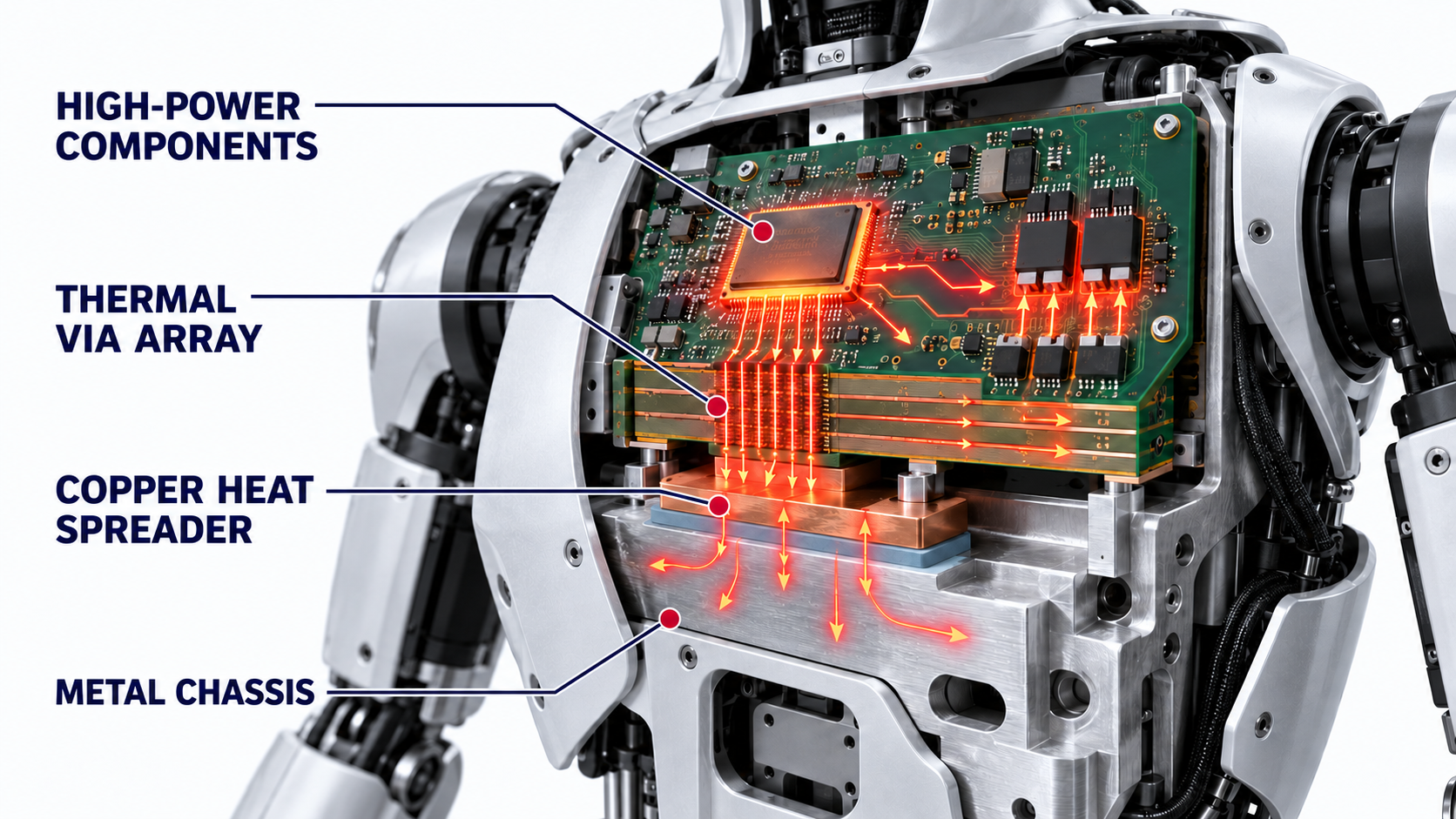
1. Thermal vias and via arrays
Thermal vias conduct heat from a component pad into internal or backside copper planes. Dense arrays are often used beneath power semiconductors, motor drivers, DC-DC converters, processors, and other bottom-terminated packages. Via diameter, pitch, plating, fill method, copper-plane connection, and proximity to the heat source all influence performance. Filled, plugged, or capped via-in-pad structures can help prevent solder wicking during assembly while supporting a short thermal path.The array should lead somewhere useful. Moving heat through the board provides limited benefit if the receiving plane cannot spread it or connect to a heat sink, enclosure, or chassis.
2. Heavy copper and optimized power planes
Heavy copper can increase current-carrying capacity, reduce voltage drop, limit resistive heating, and spread heat laterally. It can be useful for actuator power distribution, motor-control electronics, battery interfaces, and high-current conversion stages.Copper weight alone does not solve every thermal problem. Plane geometry, neck-downs, via transitions, layer connections, copper balance, and manufacturing tolerances must be reviewed together. Mixed-copper stackups may help combine high-current power layers with finer-pitch signal layers, but they require early coordination with the PCB manufacturer.
IPC-2152 is commonly used as guidance when evaluating conductor size, current, and allowable temperature rise. Actual performance should still be validated in the finished assembly and its intended operating environment.
3. Copper coin technology
A copper coin is a solid copper insert used to create a low-thermal-resistance path beneath a concentrated heat source. It can transfer heat more directly to a heat sink, chassis, or cold plate than conventional via arrays alone. This approach may be considered for localized high-power devices when space is constrained and the required vertical heat transfer exceeds what plated vias and copper planes can practically provide.4. Insulated metal substrate PCBs
An insulated metal substrate combines a conductive metal base with a thermally conductive dielectric and copper circuitry. The metal base spreads heat across a larger area and can serve as part of the cooling structure. This may be appropriate for certain power-conversion, motor-control, or high-output lighting modules within a robot. The dielectric is a critical part of the thermal path, so thermal conductivity, dielectric strength, thickness, and long-term reliability must be evaluated together.5. Component placement and heat spreading
Place heat-generating devices with the complete heat path in mind. Avoid concentrating major heat sources in a small region unless the board and mechanical design provide a deliberate way to remove that heat. Placement should account for:- Copper area available for heat spreading
- Distance from temperature-sensitive sensors and components
- Access to airflow or a mechanical heat spreader
- Routing for high-current paths
- Location of connectors and moving interconnects
- Signal-return paths and EMI control
- Assembly and inspection requirements
6. Chassis and enclosure coupling
In a compact robot, the frame or enclosure may provide a more practical heat path than airflow. Thermal interface materials, heat spreaders, mounting hardware, and controlled board-to-chassis contact can transfer heat out of the PCB assembly. This approach requires close coordination among electrical, mechanical, and thermal teams. Interface pressure, flatness, tolerance stackups, electrical isolation, vibration, serviceability, and robot movement can all affect thermal performance over time.Match the Thermal Strategy to the Robot Subsystem
| Humanoid Robot Area | Common Heat Sources | PCB Considerations |
|---|---|---|
| Torso or central compute | CPUs, GPUs, FPGAs, memory, network devices | Thermal via arrays, large copper planes, chassis coupling, high-Tg materials, controlled impedance |
| Joint and actuator modules | Motor drivers, MOSFETs, current-sense circuits | Heavy copper, short current paths, multiple vias at layer transitions, local heat spreading |
| Battery and power distribution | Battery-management circuits, converters, protection devices | Copper sizing, voltage-drop control, temperature sensing, creepage and clearance, fault-current planning |
| Head and perception systems | Cameras, processors, communications | Local hot-spot control, low-noise power, heat isolation from sensors, compact HDI stackups |
| Hands and distal limbs | Compact drivers, sensors, communications | Low mass, limited airflow, rigid-flex integration, careful separation of bend areas from heat sources |
Materials and Stackup Decisions
The stackup determines how heat and current travel through the board. Copper thickness, plane placement, dielectric thickness, resin system, glass transition temperature, thermal conductivity, and coefficient of thermal expansion all affect performance and reliability. High-Tg laminates may be appropriate when the board will experience elevated operating temperatures or repeated thermal excursions. Low-loss materials may also be needed for high-speed compute and communication circuits. In those cases, the design must balance thermal performance, signal integrity, manufacturability, availability, and cost.
Rigid-flex designs introduce additional considerations. Heat sources should generally be kept out of bend regions, and copper distribution must support both electrical performance and mechanical movement. The rigid-to-flex transition, bend radius, dynamic-flex requirements, and nearby thermal structures should be reviewed before layout is complete.
Validate the Design Under Real Operating Conditions
Thermal analysis should continue beyond simulation. Validate the assembled robot or representative subsystem under realistic loads, movement profiles, and enclosure conditions.
A useful validation plan can include:
- Thermal simulation before layout release
- Thermocouple measurements at critical components and PCB locations
- Infrared imaging to locate unexpected hot spots
- Testing during sustained and peak actuator loads
- Monitoring processor performance for thermal throttling
- Voltage-drop and current measurements across high-current paths
- Thermal cycling with powered operation where appropriate
- Vibration or motion testing combined with temperature exposure
- Comparison of prototype data with production-intent materials and assembly processes
Testing should reflect how the robot will be used. Bench testing with covers removed, external fans operating, or actuators unloaded may hide problems that appear in the final system.
Review Manufacturability Before Layout Is Finalized
Thermal PCB features can affect drilling, plating, lamination, etching, solder-mask application, assembly, and inspection. Early collaboration with the PCB manufacturer helps confirm that the proposed construction can be produced reliably. Before release, review:
- Copper weights and mixed-copper requirements
- Trace and plane geometry for high-current paths
- Thermal-via diameter, pitch, aspect ratio, and fill or cap requirements
- Via-in-pad structures beneath bottom-terminated components
- Copper coin geometry and mechanical interfaces
- IMS material and dielectric requirements
- Stackup symmetry and copper balance
- Controlled-impedance requirements
- Rigid-flex transitions and bend regions
- Finished thickness and enclosure tolerances
- Prototype-to-production material availability
- Inspection, testing, documentation, and traceability requirements
This review can identify thermal risks and manufacturing conflicts while changes are still easier and less expensive to make.
Building a Reliable Path from Prototype to Production
Humanoid robots need PCBs that can manage power and heat while surviving motion, vibration, compact packaging, and repeated thermal cycling. The strongest designs treat the PCB as an active part of the thermal system, not simply a platform for components.
AdvancedPCB manufactures thermal-management PCBs using capabilities that include thermal via arrays, via-in-pad structures, heavy copper, mixed-copper stackups, copper coin technology, IMS constructions, multilayer boards, HDI features, and controlled-depth structures. Our engineering and manufacturing teams can review stackups, copper distribution, via structures, materials, and manufacturability requirements early in development.
By aligning electrical, thermal, mechanical, and manufacturing decisions before fabrication, robotics teams can reduce redesign risk and create a more consistent path from prototype through production.
Learn more about AdvancedPCB thermal-management PCB capabilities
Talk with our robotics PCB team
.png)
AdvancedPCB
Related Posts
Why Do PCBs Have an Even Number of Layers?
Heavy Copper PCBs for Automotive Electronics: Design Considerations