Single-Sided vs. Double-Sided vs. Multilayer PCBs: How to Choose

By the AdvancedPCB Content Team | Originally published January 3, 2013 | Updated October 14, 2026
When you are in the process of building your Printed Circuit Boards, it is important to understand the differences between types of Printed Circuit Boards so you choose the one that will be best for your application. AdvancedPCB is here to help you get the Printed Circuit Boards you need and offers tips to get you started in the right direction. Single-sided boards are made from rigid laminate with copper on one side of varying thickness. Double-sided boards differ in that they have copper on both sides of the laminate. A multi-layer PCB has copper foil on the top and bottom and “inner layer” cores. These multi-layer PCBs are commonly used in more complex electronic designs that require higher density and improved signal integrity. Each type of PCB has its own unique advantages, so work with an AdvancedPCB expert to get the one that is best for you.
What is a Single-Sided PCB?
Single-sided Printed Circuit Boards are typically used for simpler, lower-cost applications where components and routing can be kept on one side of the board. These Printed Circuit Boards are ideal for straightforward consumer products, basic power supplies, and other designs where minimal complexity is required. Because they use copper on only one side of the laminate, they are easier to manufacture and often provide a more economical solution for high-volume production.
What is a Double-Sided PCB?
Double-sided Printed Circuit Boards add flexibility by allowing traces and components on both sides of the board. This makes it easier to route more complex circuits without dramatically increasing the overall size of the PCB. Double-sided Printed Circuit Boards are widely used in industrial controls, power management systems, and many types of consumer electronics that require moderate complexity and reliability. With plated through-holes connecting the two layers, designers can achieve more compact layouts than with single-sided options.
What is a MultiLayer PCB?
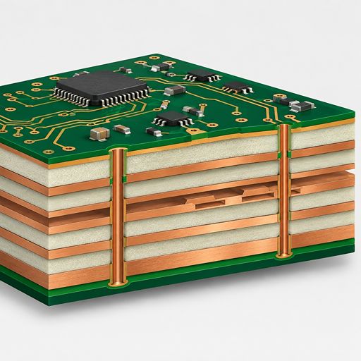
Multilayer PCBs take this a step further by stacking several layers of copper and insulating material together. These multi-layer PCBs can include dedicated power and ground planes, as well as multiple signal layers, which help reduce noise, improve electromagnetic compatibility, and support very dense component placement. Printed Circuit Boards with four, six, or more layers are common in advanced applications such as telecommunications equipment, high-speed computing, and compact consumer devices like smartphones and tablets. By carefully selecting the number of layers and their arrangement, designers can optimize performance while maintaining a small footprint.
Most multilayer boards use an even number of layers, such as 4, 6, 8, or 10. A balanced, symmetric stackup reduces bow and twist during lamination and reflow. Internal layers are often dedicated to power and ground planes, which shortens return paths, lowers noise, and makes controlled impedance routing practical.
Multilayer boards can use through-hole vias, blind and buried vias that connect only selected layers, and back drilling to remove unused via stubs in high-speed designs. Designs that add laser-drilled microvias and multiple sequential lamination cycles fall into the HDI PCB category.
Single-Sided vs. Double-Sided vs. Multilayer PCBs at a Glance
| Single-Sided | Double-Sided | Multilayer | |
|---|---|---|---|
| Also called | SIngle-layer PCB | Two-layer PCB | Multi-layer PCB |
| Copper layers | 1 | 2 | 3 or more, usually an even number |
| Layer interconnect | None | Plated through holes and vias | Through-hole, blind and buried vias |
| Routing density | Low | Moderate | High |
| Component placement | Components on one side | Both sides | Both sides |
| Power and ground planes | No | Partial ground pour | Dedicated internal planes |
| Controlled impedance | Not practical | Possible, with limits | Standard practice |
| Relative cost | Lowest | Low to moderate | Moderate to high, rises with layer count |
| Typical applications | Power supplies, LED lighting, sensors, simple controls | Industrial controls, automotive modules, instrumentation, power conversion | Aerospce and defense, medical, data centers, telecom, robotics |
How to Choose the Right PCB Type
The right board type depends on four factors. In most designs, one of them sets the minimum layer count and the others confirm it.Circuit Complexity and Component Density
Count the connections, not just the components. A circuit with a few dozen nets and through-hole parts often fits on a single-sided board. Once the layout needs more than a handful of jumpers, a second copper layer is usually cheaper overall. Fine-pitch BGAs, high pin-count processors, and FPGAs generally require multilayer boards to escape-route every pin.Operating Frequency and Signal Integrity
High-speed and high-frequency signals need a continuous reference plane directly beneath the trace and tightly controlled trace geometry. Two-layer boards can approximate this with a ground pour or coplanar waveguide routing, but multilayer stackups provide solid internal planes that keep impedance predictable and limit crosstalk and EMI.Board Size and Available Space
If the enclosure is fixed, the board area is fixed. Adding layers is often the only way to fit the required routing into a smaller footprint, which is why compact products in medical, aerospace, and robotics applications rely on multilayer construction.Budget and Production Volume
Fabrication cost rises with each layer and each lamination cycle. For high-volume products with simple circuits, a single-sided or double-sided board keeps unit cost low. For complex designs, a multilayer board can reduce total cost by shrinking the board, simplifying assembly, and avoiding signal integrity rework.Designing Your PCB with Software from AdvancedPCB
You can create your custom PCB with PCB Artist software from AdvancedPCB. This free tool allows you to design your Printed Circuit Boards and get your Gerber files checked before placing your order so you can work out any manufacturability issues that may arise beforehand. By using PCB Artist, you can experiment with different stackups, including single-sided, double-sided, and multi-layer PCBs, to determine which configuration best suits your project requirements. The software makes it easy to visualize how traces, vias, and components will be arranged across the layers of your Printed Circuit Boards.
Once your design is complete, AdvancedPCB’s engineering team can review your files and provide feedback on material selection, layer count, and other critical aspects of your multi-layer PCBs or simpler designs. This collaborative approach helps ensure that your Printed Circuit Boards are not only functional on paper but also optimized for real-world manufacturing and long-term reliability. Contact a representative at AdvancedPCB today for more information and to learn how their expertise can support your next project.
.png)
AdvancedPCB
Multilayer PCB FAQ'S
Related Posts
Why Do PCBs Have an Even Number of Layers?