Heavy Copper PCBs for Automotive Electronics: Design Considerations
Automotive electronics combine power delivery, sensing, and control within demanding packaging and operating environments. Heavy copper PCBs can help support selected circuits that carry higher currents or require improved heat distribution, across conventional, hybrid, and electric vehicles.
Getting those benefits requires more than increasing copper weight. Engineers must coordinate conductor geometry, thermal paths, spacing, and stackup with the manufacturing process. This article explains the key considerations before releasing an automotive power electronics PCB for fabrication.
This guide builds on AdvancedPCB’s Heavy Copper in PCB Design article and applies its principles to automotive electronics development.
Specify Copper Thickness Clearly
Copper weight describes the amount of copper per unit area and is commonly expressed in ounces per square foot. AdvancedPCB’s foundational article, Heavy Copper in PCB Design, describes heavy copper constructions in the 5–19 oz/ft² range, while noting that definitions vary.
For a fabrication drawing, a label such as “heavy copper” is not enough. Identify the copper requirement for each layer and clarify whether it refers to starting foil or finished copper thickness. Discuss hole-wall plating requirements separately rather than assuming they match the conductor thickness.
Match Copper to the Circuit’s Job
Heavy copper is a design option for selected automotive power circuits. The following applications provide useful starting points for that evaluation:
| Application | Circuits to evaluate |
|---|---|
| Power distribution | Selected paths supplying and switching vehicle electrical loads |
| Motor control | Power stages driving pumps, fans, and other electric motors |
| Body and comfort systems | Selected actuator and heating power circuits |
| Lighting | Driver and power circuitry with demanding thermal requirements |
| Hybrid and electric powertrains | Selected charging, DC-DC conversion, and inverter power paths |
These are applications for evaluation, not a statement that every board in these systems requires heavy copper. Monitoring and control circuitry may have different copper needs from the power stage.
In some traction inverter architectures, busbars and ceramic power-module substrates carry substantial power alongside PCBs. Start by identifying which currents actually travel through the PCB, then select its copper construction accordingly.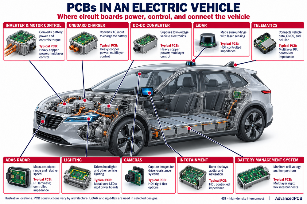
PCB applications in an electric vehicle. This illustration shows a range of PCB technologies used throughout the vehicle. Heavy copper is an option for selected high-current power circuits; other modules may use different constructions. Many of these electronic functions also appear in conventional and hybrid vehicles.
Size the Complete Current Path
Increasing copper thickness increases a conductor’s cross-sectional area. For the same material, length, and width, that reduces resistance and the resistive heating produced at a given current. Width and length still matter, as do vias connecting the layers. A practical review should examine the entire route from the input connection to the load. Pay attention to narrow necks at pads, layer transitions, and via arrays. A broad copper region does not remove a bottleneck elsewhere in the path. For switching converters, current-loop geometry also matters. Copper thickness and compact loop routing should be considered together when evaluating efficiency and layout performance.Plan How Heat Leaves the Board
Heavy copper can help distribute heat, but the thermal design needs a path beyond the component. Copper planes and thermal vias can move heat through the PCB, while the package, board construction, and cooling arrangement determine the overall result.
Review the component manufacturer’s thermal-pad recommendations, the connection to internal planes, and the interface to any external cooling structure. Validate temperature rise under representative operating conditions. Increasing copper weight alone does not establish that the board will remain within its temperature limits.
Allow for Heavy Copper Manufacturing Rules
Thicker copper changes the limits of the etching process. Minimum conductor widths and isolation gaps must be reviewed for the selected copper thickness; fine features that work on a thinner copper layer may require adjustment. Before completing the layout, ask your fabricator to confirm:
- Minimum trace widths and copper-to-copper spacing for each layer
- Pad clearances and annular-ring requirements
- Starting and finished copper thicknesses
- Drill sizes and plating requirements
- Solder mask requirements around dense features
Manufacturing spacing and electrical insulation spacing serve different purposes. Meeting an etching limit does not, by itself, establish that a high-voltage design has adequate insulation. Specify the applicable electrical requirements in addition to fabrication rules.
Use IPC Standards to Define Design and Fabrication Requirements
IPC standards provide useful references when specifying automotive power electronics PCBs. IPC-2152 offers guidance on selecting conductor dimensions based on required current and acceptable temperature rise. Engineers should apply that guidance alongside the board’s construction, cooling conditions, and operating requirements.
IPC-2221 and IPC-2222 address general and rigid printed board design considerations, while IPC-6012 establishes qualification and performance requirements for rigid boards. Automotive programs may also specify the applicable automotive addendum to IPC-6012.
Identify the required standards, revisions, performance class, and customer-specific requirements in the fabrication documentation, and confirm them with the manufacturing team before release.
Combine Copper Weights Thoughtfully
A board may need substantial copper for power distribution and finer routing for control electronics. Discuss whether different copper weights on separate layers can meet those needs. Constructions using different thicknesses within the same layer require a specific manufacturing review and should not be treated as interchangeable with a mixed-weight stackup.
Copper distribution also affects mechanical stability. Uneven copper coverage or an asymmetric multilayer construction can contribute to bow and twist. Review copper coverage and the stackup together, particularly when large power regions sit beside sparsely routed control areas.
Review the Design Before Release
AdvancedPCB’s automotive engineering support covers stackup development, material selection, copper weight, controlled impedance, thermal management, via structures, and design for manufacturability.
To make that discussion productive, provide fabrication data, a proposed stackup, layer-specific copper requirements, operating current and voltage, thermal constraints, and expected quantities. Identify requirements that must remain fixed and decisions that are still open for review. The goal is a construction that meets the application’s needs and can be manufactured consistently as the program grows.
Plan the Path from US Prototypes to Global Production
AdvancedPCB supports US prototype builds and higher-volume PCB production through Global Solutions. Its team manages the transfer of reviewed manufacturing files to vetted overseas partner facilities matched to the board’s technology and production requirements.
Your dedicated AdvancedPCB representative remains the point of contact for production coordination. For heavy copper programs, discuss the planned production route early so copper requirements, materials, and manufacturing constraints can be reviewed before the design is released.
Explore AdvancedPCB’s automotive capabilities and discuss the right construction for your next power electronics board.
.png)
AdvancedPCB
Related Posts

Built for the Factory Floor
Is Your Robotic PCB Design Ready for Manufacturing?