


Double-Sided PCB Manufacturing
Two-layer rigid circuit boards with plated through holes, built in the U.S. for prototype and production programs.
This page explains double-sided PCBs, how they are built, and when a two-layer board is the right fit for a design. Topics include double-sided PCB construction and plated through holes, through-hole and surface mount assembly options, advantages and trade-offs, where to find our manufacturing capabilities, common applications, design considerations, and frequently asked questions.
What Is a Double-Sided PCB?
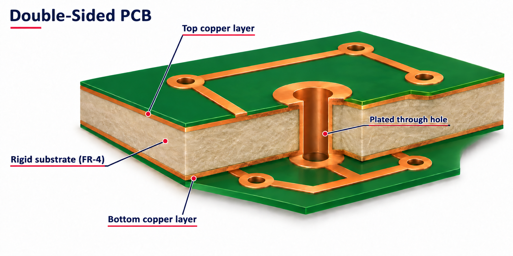
A double-sided PCB, also called a two-layer PCB, has copper on both the top and bottom of a rigid substrate. Plated through holes connect circuits on one side to the other, which lets traces cross over each other and doubles the available routing area compared with a single-sided board.
During fabrication, holes are drilled through the panel, coated with electroless copper, and then built up with electrolytic copper plating. The result is a conductive barrel that carries signals and current between layers and strengthens through-hole solder joints.
Advantages and Limitations of Single-Sided PCBs
Advantages
- Twice the routing area of a single-sided board
- Components can be placed on both sides for a smaller footprint
- Plated through holes improve joint reliability
- Lower cost than multilayer boards for moderately complex circuits
- Room for a partial ground pour to improve noise performance
Limitations
- More process steps than single-sided, including drilling and plating
- Limited options for dedicated power and ground planes
- Controlled impedance is possible but requires wide traces on standard thicknesses
- High-speed digital and dense BGA designs usually need four or more layers
Double-Sided PCB Capabilities
Detailed specifications for double-sided PCBs, including board thickness, copper weights, trace and space, drilling, and impedance tolerances, are listed on our Manufacturing Capabilities page. Capabilities can be viewed by facility.
Double-Sided PCB Applications
Single-sided boards remain the practical choice for circuits with low component counts and simple signal paths.
- Industrial controls and motor drives
- Automotive body, lighting, and accessory modules
- HVAC and power conversion equipment
- Instrumentation and test equipment
- Audio amplifiers and signal conditioning
- LED lighting and power distribution
Double-Sided PCB Design Considerations
- Use the bottom side for ground.
- Place vias with intent. Stitching vias tie ground pours together, and via placement affects both routing and thermal behavior.
- Add thermal relief where needed. Pads connected to large copper areas need relief spokes so they solder reliably.
- Check drill and annular ring sizes. Specify finished hole sizes and pad diameters that meet your IPC class.
- Understand impedance limits.
- Know when to move to multilayer. Dense routing, fine-pitch BGAs, high-speed interfaces, or tight EMI requirements usually justify a multilayer PCB.