


Multilayer PCB Manufacturing
Two-layer rigid circuit boards with plated through holes, built in the U.S. for prototype and production programs.
This page explains double-sided PCBs, how they are built, and when a two-layer board is the right fit for a design. Topics include double-sided PCB construction and plated through holes, through-hole and surface mount assembly options, advantages and trade-offs, where to find our manufacturing capabilities, common applications, design considerations, and frequently asked questions.
What Is a Multilayer PCB?
A multilayer PCB has three or more copper layers bonded into a single rigid board. Inner layers are imaged and etched on thin cores, stacked with prepreg, and laminated under heat and pressure. The panel is then drilled, plated, and finished like a double-sided board, with plated holes connecting the layers.
Most multilayer boards use an even number of layers. A balanced, symmetric stackup helps prevent bow and twist during lamination and assembly.
How Multilayer PCBs Are Built
- Inner layer imaging and etching
- Automated optical inspection (AOI) of inner layers
- Oxide or bond treatment for layer adhesion
- Layup and lamination of cores and prepreg
- Drilling, including back drilling where specified
- Copper plating of holes and vias
- Outer layer imaging, etching, solder mask, and surface finish
- Electrical test and final inspection
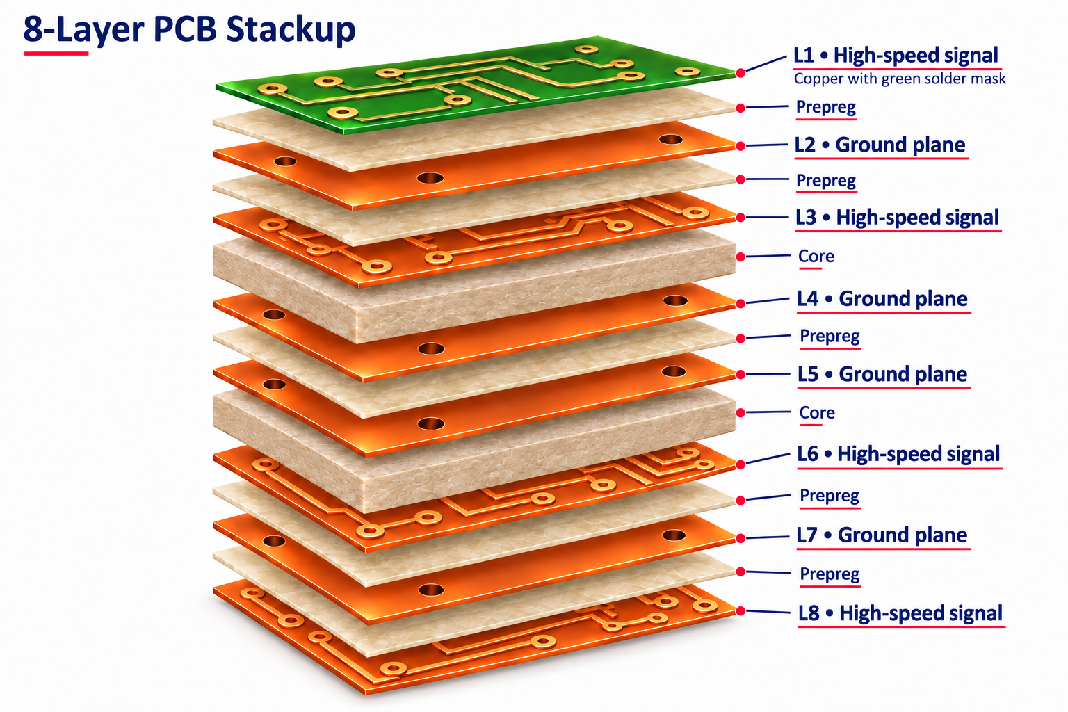
Common Multilayer PCB Layer Counts
| Layer Count | Typical Stackup | Common Uses |
|---|---|---|
| 4 layers | Signal, ground, power, signal | Embedded controllers, industrial and automotive electronics |
| 6 layers | Added inner signal layers with reference planes | Mixed-signal designs, improved EMI performance |
| 8-10 layers | Multiple signal layers between ground planes | FPGAs, processors, high-speed digital |
| 12 layers and up | High layer count with controlled impedance pairs | Data center, networking, aerospace and defense systems |
Via Structures for Multilayer PCBs
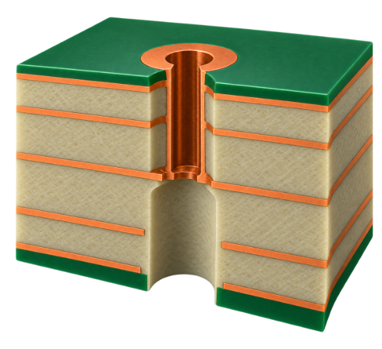
Back Drilling
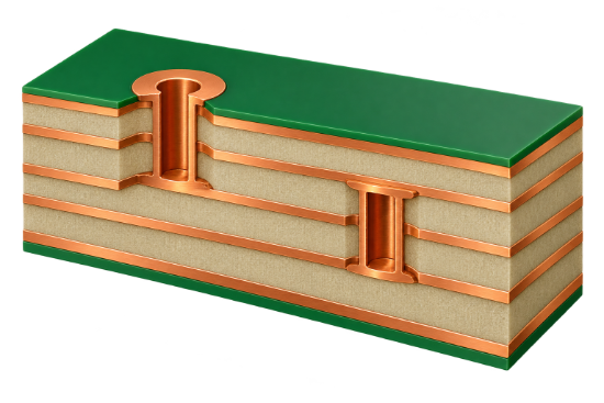
Blind and Buried Vias
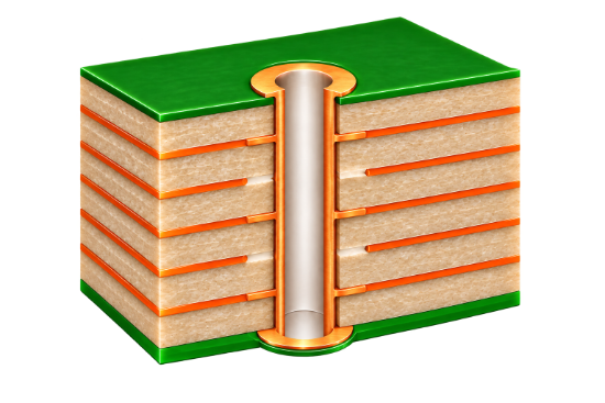
Through-Hole Vias
.png?resizemode=force&maxsidesize=550)
Via-In-Pad
Read "Understanding Blind Buries Vias PCB for High-Density Designs" for more information on vias
Stackup Design and Controlled Impedance
Stackup decisions set the electrical performance of a multilayer board. Our engineers help define layer order, dielectric thickness, copper weights, and trace geometry to meet impedance targets for single-ended and differential signals. Impedance is verified with time domain reflectometry (TDR) on test coupons built with each panel.
Multilayer PCB Materials
- Standard and high-Tg FR-4 for general multilayer builds
- Low-loss and high-speed laminates for fast digital interfaces
- Rogers and PTFE laminates for RF layers, including hybrid FR-4 and RF stackups. See RF and Microwave PCBs.
- Materials selected for lead-free assembly and thermal cycling reliability
Multilayer PCB Capabilities
Detailed specifications for multilayer PCBs, including board thickness, copper weights, trace and space, drilling, and impedance tolerances, are listed on our Manufacturing Capabilities page. Capabilities can be viewed by facility.
Multilayer PCB Applications
- Aerospace and defense: Radar, avionics, communications, and mission computers
- Medical technologies: Imaging, diagnostics, and patient monitoring systems
- Data center and AI infrastructure: Servers, accelerators, and storage
- Telecommunications and networking: Switches, routers, and base station hardware
- Robotics: Motion control, vision, and embedded compute
- Industrial: Automation controllers, drives, and test systems