


RF PCB: What It Is and How It Works
Posted
11/13/2026
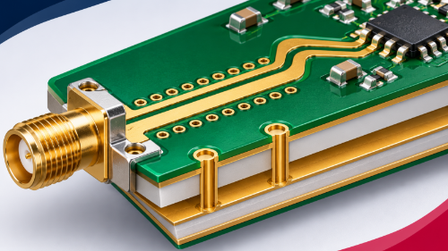
An RF PCB (radio frequency printed circuit board) is designed to carry radio frequency signals while controlling impedance, signal loss, and interference. RF PCBs are used in wireless communications, radar, satellite systems, medical electronics, and other applications that transmit or receive high-frequency signals.
Unlike conventional low-frequency PCB designs, RF circuits often require careful control of transmission-line geometry, dielectric properties, and signal return paths. These factors help maintain predictable performance as signals travel between components, antennas, and connectors.
At higher frequencies, PCB traces can behave as transmission lines rather than simple electrical connections. Their dimensions, surrounding materials, and reference planes influence how signals propagate.
RF PCBs may be rigid, flexible, or multilayer. Depending on the application, they can use conventional FR-4, specialized low-loss laminates, or combinations of different materials.
Three characteristics are particularly important:
Not every RF PCB requires specialty materials. The appropriate construction depends on the design's performance requirements.
For a more detailed explanation of materials and manufacturing considerations, read RF Microwave PCB Design: Materials, Layout, and Manufacturing Best Practices.
RF PCB manufacturing requires close attention to the physical characteristics that affect signal performance.
Important considerations include dielectric thickness, finished trace dimensions, copper roughness, laminate properties, and layer registration.
As operating frequencies increase, small manufacturing variations can become more significant. Engineers and PCB manufacturers must work together to ensure the finished board reflects the intended electrical design.
For example, a change in dielectric thickness can affect characteristic impedance, while conductor roughness can contribute to signal loss.
Manufacturing requirements should therefore be established before production, particularly for designs using specialized RF laminates or controlled-impedance structures.
Our U.S.-based manufacturing capabilities include Rogers and Taconic RF laminates, controlled impedance, multilayer constructions, hybrid stackups, and advanced via technologies.
We work with engineering teams to review manufacturing requirements and help identify potential issues before fabrication.
Looking for an RF PCB manufacturer? Explore our RF and Microwave PCB Manufacturing Services to review capabilities and request a quote.
Unlike conventional low-frequency PCB designs, RF circuits often require careful control of transmission-line geometry, dielectric properties, and signal return paths. These factors help maintain predictable performance as signals travel between components, antennas, and connectors.
What Is an RF PCB?
An RF PCB is a circuit board designed for electronic systems that operate at radio frequencies. The RF spectrum extends from approximately 3 kHz to 300 GHz, although many practical RF PCB applications operate in the MHz and GHz ranges.At higher frequencies, PCB traces can behave as transmission lines rather than simple electrical connections. Their dimensions, surrounding materials, and reference planes influence how signals propagate.
RF PCBs may be rigid, flexible, or multilayer. Depending on the application, they can use conventional FR-4, specialized low-loss laminates, or combinations of different materials.
How Does an RF PCB Work?
An RF PCB connects electronic components while providing controlled paths for high-frequency signals. For example, in a wireless communication device, an RF signal may travel from a transceiver through filters and amplifiers before reaching an antenna. The PCB interconnections must support the required impedance and limit unwanted reflections or losses.Three characteristics are particularly important:
- Controlled impedance: Helps signals travel between components without excessive reflections.
- Low signal loss: Reduces the energy lost as signals move through the PCB.
- Signal isolation: Helps prevent interference between nearby RF circuits and other electronics.
Where Are RF PCBs Used?
RF PCBs support a wide range of technologies that depend on wireless communication, sensing, and high-frequency signal processing.| Application | How RF PCBs Are Used |
|---|---|
| Wireless communications | Signal routing in Wi-Fi, cellular, and telecomunications equipment |
| Radar systems | RF signal paths for transmitting, receiving, and processing radar signals |
| Satellite communications | RF circuitry in communication payloads and ground equipment |
| Aerospace and defense | Radar, navigation, communications, and electronic sensign systems |
| Automotive electronics | Radar sensors used in advanced driver assistance systems |
| Medical technology | RF electronics in selected imaging, monitoring, and therapeautic equipment |
| Test and measurement | Signal generation, analysis, and high-frequency instrumentation |
Each application has different electrical, environmental, and manufacturing requirements.
RF PCB vs. Standard PCB
RF PCBs and conventional PCBs use many of the same fabrication processes. The main difference is the attention required to maintain high-frequency electrical performance.
| Feature | Conventional PCB | RF PCB |
| Primary design focus | Electrical connectiviity and circuit functionality | Signal transmission, impedance, loss, and isolation |
| Materials | Commonly standard FR-4 | FR-4 or specialized RF laminates |
| Trace geometry | Based on current, spacing, and signal requirements | Often requires controlled transmission-line dimensions |
| Manufacturing | Standard fabrication tolerances where appropriate | Tighter control of critical RF features may be needed |
| Verification | Electrical and dimensional inspection | May include additional impedance or RF performance measurements |
Not every RF PCB requires specialty materials. The appropriate construction depends on the design's performance requirements.
For a more detailed explanation of materials and manufacturing considerations, read RF Microwave PCB Design: Materials, Layout, and Manufacturing Best Practices.
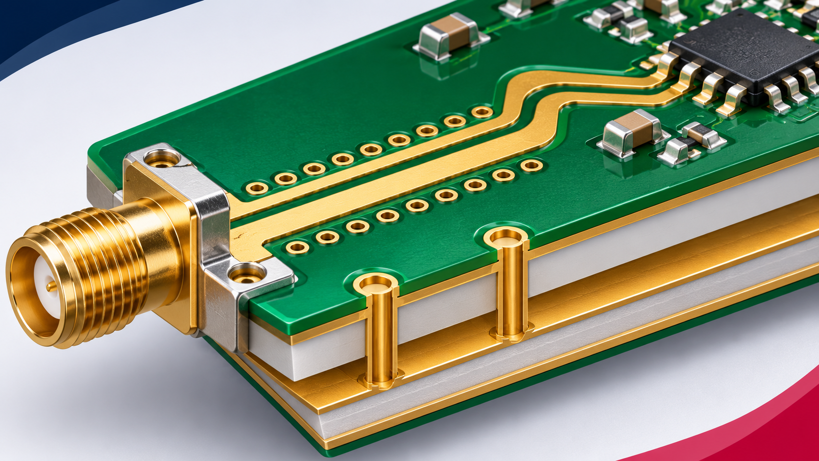 What Makes RF PCB Manufacturing Different?
RF PCB manufacturing requires close attention to the physical characteristics that affect signal performance.Important considerations include dielectric thickness, finished trace dimensions, copper roughness, laminate properties, and layer registration.
As operating frequencies increase, small manufacturing variations can become more significant. Engineers and PCB manufacturers must work together to ensure the finished board reflects the intended electrical design.
For example, a change in dielectric thickness can affect characteristic impedance, while conductor roughness can contribute to signal loss.
Manufacturing requirements should therefore be established before production, particularly for designs using specialized RF laminates or controlled-impedance structures.
What Should Engineers Consider Before Ordering an RF PCB?
Before sending an RF PCB design for fabrication, engineers should identify:- Operating frequency and bandwidth
- Required characteristic impedance
- Acceptable signal loss
- Preferred laminate materials
- Board thickness and stackup requirements
- Connector and via requirements
- Operating temperature and environmental conditions
- Inspection and testing requirements
RF PCB Manufacturing at AdvancedPCB
AdvancedPCB manufactures RF and microwave printed circuit boards for demanding applications, including wireless infrastructure, radar, aerospace, and satellite communications.Our U.S.-based manufacturing capabilities include Rogers and Taconic RF laminates, controlled impedance, multilayer constructions, hybrid stackups, and advanced via technologies.
We work with engineering teams to review manufacturing requirements and help identify potential issues before fabrication.
Looking for an RF PCB manufacturer? Explore our RF and Microwave PCB Manufacturing Services to review capabilities and request a quote.
FAQs for RF PCBs
What is the difference between an RF PCB and a microwave PCB?
Can FR-4 be used for RF PCB designs?
What does RF PCB stand for?
What materials are used in RF PCBs?
Why is controlled impedance important in RF PCBs?
Related Posts
Why Do PCBs Have an Even Number of Layers?
Reasons why PCBs typically have an even number of layers
Why Do PCBs Have an Even Number of Layers?
Read More

AdvancedPCB Achieves CMMC Certification
AdvancedPCB has achieved CMMC Level 2 Status
AdvancedPCB Achieves CMMC Certification
Read More
Browse
All Categories
Recent Posts
View Recent Posts