

Blog

The PCB Fabrication Process
A step-by-step look at how PCBs are manufactured.
The PCB Fabrication Process
Read More
Editor's Picks

How to Keep Your Schematic and PCB Layout in Sync
Learn how to prevent schematic-to-PCB mismatches
How to Keep Your Schematic and PCB Layout in Sync
Read More

5 PCB Failures That Ground Drones, and How to Design Against Them
Learn the most common PCB failures in drone electronics, including vibration fatigue, thermal issues, RF interference, and thermal cycling, plus design strategies and IPC standards that improve UAV reliability.
5 PCB Failures That Ground Drones, and How to Design Against Them
Read More

RF Microwave PCB Design: Materials, Layout, and Manufacturing Best Practices
Learn RF microwave PCB design fundamentals including materials, impedance control, stackups, routing, testing, and manufacturing best practices.
RF Microwave PCB Design: Materials, Layout, and Manufacturing Best Practices
Read More
View All

PCBs for Robotics: Enhancing Performance and Functionality
Explore pcbs for robotics designed for automation, durability, and precision in various applications. Enhance your projects today.
PCBs for Robotics: Enhancing Performance and Functionality
Read More

ENIG PCB Finish
Learn what an ENIG PCB finish is, how it works, and when to use it. Compare ENIG vs other PCB finishes for reliability, solderability, and performance.
ENIG PCB Finish
Read More

Space-Grade PCBs: Requirements, Materials, Standards, and Design Priorities
Learn how PCBs are built and tested for space missions. Explore materials, rigid vs flex designs, satellite PCBs, and how to source space-grade boards.
Space-Grade PCBs: Requirements, Materials, Standards, and Design Priorities
Read More

Rigid-Flex PCB Material Guide for Design Engineers
Learn how to select rigid-flex PCB materials including polyimide, copper, and adhesives. Improve reliability, flexibility, and performance in your designs.
Rigid-Flex PCB Material Guide for Design Engineers
Read More

AdvancedPCB Strengthens HDI Process Control with New AOI Investment in Chandler, AZ Facility
AdvancedPCB enhances HDI PCB manufacturing with new AOI inspection technology, improving precision, yield, and reliability for aerospace, AI, and advanced computing applications. Keywords:
AdvancedPCB Strengthens HDI Process Control with New AOI Investment in Chandler, AZ Facility
Read More

5 Reasons ‘Working’ Schematics Fail During PCB Layout
Learn why working schematics fail during PCB layout. Discover common issues with net naming, power symbols, connectors, and hierarchy, and how to avoid costly errors.
5 Reasons ‘Working’ Schematics Fail During PCB Layout
Read More
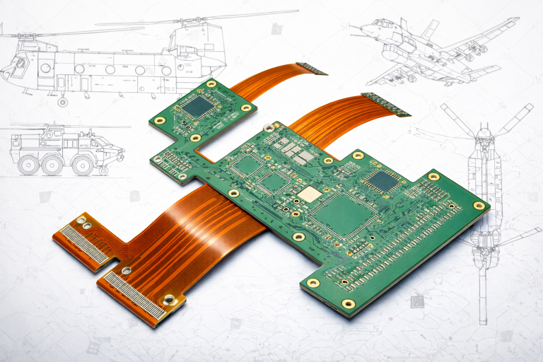.png?resizemode=force&maxsidesize=1226 "Rigid-flex PCBs for Aerospace & Defense")
The Role of Rigid-Flex PCBs in Aerospace & Defense Prototypes
Explore the role of rigid-flex pcbs in aerospace & defense prototypes, highlighting their advantages and best design practices.
The Role of Rigid-Flex PCBs in Aerospace & Defense Prototypes
Read More

How Integrated PCB Fabrication and Prototype Assembly Improves Speed and Program Control
Learn how integrated PCB fabrication and assembly improves fast PCB assembly timelines, supports urgent PCB assembly services, and increases reliability for engineering teams and buyers sourcing PCBA.
How Integrated PCB Fabrication and Prototype Assembly Improves Speed and Program Control
Read More

Rigid PCB Uses: Applications, Design Considerations, and Manufacturing Practices
Learn what rigid PCBs are, where they are used, and how they are designed and manufactured. This guide explains rigid PCB materials, applications, stackup design, IPC standards, and fabrication processes.
Rigid PCB Uses: Applications, Design Considerations, and Manufacturing Practices
Read More
Browse
All Categories